
Rebuilt Feedthroughs
Rigaku rebuilds ferrofluid feedthroughs for all leading manufacturers and offers a warranty on rebuilt units. Most parts are stocked in inventory for fast turnaround. Learn More.
Rigaku Vacuum Products
E-mail: vacuum-info@rigaku.com
Phone: 603-890-6001
|
No One Can Shut You Down Faster Than Comdel
Comdel's new Arc Detect Fast Shutdown works within the matching network and power supply, providing automatic shutdown of the RF to minimize arc damage. Learn more.
Comdel
11 Kondelin Road
Gloucester, MA 01930
Tel: 978-282-0620 or 800-468-3144
Fax: 978-282-4980
www.comdel.com
info@comdel.com
|
MDC's Bundled Engineered Solutions
MDC offers virtually every component required for vacuum coating applications. With MDC's standard chamber line you have the advantage of bundling these high quality pieces together without hours or weeks of special engineering. More...
MDC
engineered process solutions
www.mdcvacuum.com
|
|
From AR Coatings to Notch Filters, and from TCOs to DBRs, Evatec offers customized coating platforms and complete process solutions based on enhanced evaporation and sputter.
Phone: (603) 669-9656
www.evatecnet.com
E-Mail:infoNA@evatecnet.com
|
Measure Thin Film Deposition
with DektakXTTM
Bruker's new DektakXTTM stylus profiler monitors thin film deposition and etch systems with the industry's best measurement repeatability (<5Å). Find out how to better control your thin film process development faster, easier and more accurately. Learn More.
Bruker Corporation
520-741-1044
productinfo@bruker-nano.com
|

Large Throttle Valves
Throttle Valves with ports as large as 630 mm, ISO-630 or ANSI 24 inch. Also any flange style as small as NW-25. Aluminum, steel or stainless steel.
Phone: 800-426-9340
Web: vacuumresearch.com
|
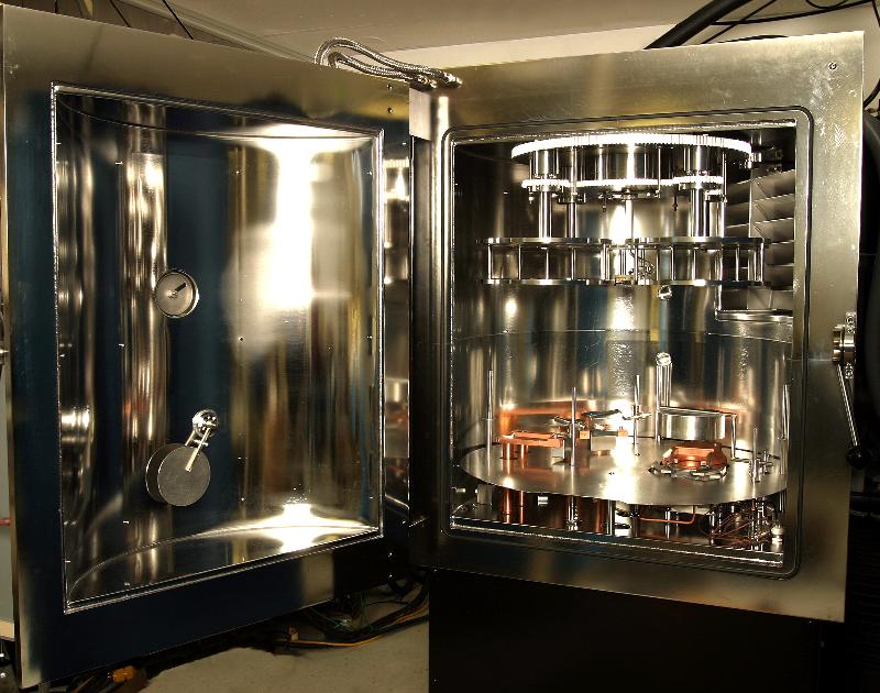
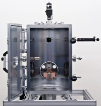
Dynavac produces a wide range of thin film deposition systems that include electron beam, thermal evaporation, sputtering and ion-assist. Our reputation is built upon quality, reliability, and excellent customer relations.
Telephone: 781-740-8600 |
 Speed pump-down and vacuum performance with RediVac™ Fasteners and Seals from UC Components Inc. Speed pump-down and vacuum performance with RediVac™ Fasteners and Seals from UC Components Inc.
|
Evans Analytical Group (EAG) is the leading global provider of high quality surface analysis and materials characterization services to the films and coatings industry.
Evans Analytical Group
1.800.366.3867
|

Solid Sealing Technology designs and manufactures hermetic assemblies using metalizing, brazing and glass-ceramic sealing including standard and custom Feedthroughs/Connectors for extreme environments and UHV.
Contact:
Ph: 518-874-3600
Fax: 518-874-3610
info@solidsealing.com
|

Thin-Films Research is prepared to meet your custom thin-film coating requirements. Using state-of-the-art equipment and over 40 years of experience, Thin-Films Research offers technology for the electro-optics, semiconductors, sensors & medical electronic industries. Learn More
Thin-Films Research, Inc.
270 Littleton Road
Westford, MA 01886
Phone: 978-692-9530
Fax: 978-692-9531
E-Mail: sales@thinfilmsresearch.com |

Leak Detector with Wireless Remote
The rugged and easy to use
SmartTestTM helium leak detector is available with a wireless remote. It detects leaks down to 5x10-12 mbar l/s. Learn More.
Pfeiffer Vacuum, Inc.
24 Trafalgar Square
Nashua, NH 03063-1988
Phone: 603-578-6500
www.pfeiffer-vacuum.com
smarttest@pfeiffer-vacuum.com
|
EQP Mass and Energy Analyser for Plasma Diagnostics
- Plasma ion analyser for +ve and -ve ion analysis
- Neutrals and neutral radical detection
- For correlation of plasma parameters with film quality Learn More
E-mail address: info@hiden.co.uk
Phone: +44 [0] 1925 445225 (UK)
or [1] 734 542 6666 (USA)
Website:www.HidenAnalytical.com
|

VAT manufactures high quality vacuum valves for a variety of applications. Products include: gate, angle, fast-closing, transfer, pendulum, throttle, pressure control, all-metal and customized valves. Learn more.
Contact Us:
Phone: 781-935-1446
or 800-935-1446
E-Mail: US@vatvalve.com
|

Capacitance Manometers that Last
...Up to 3x Longer
The rugged design of the Brooks XacTorr handles byproduct build-up, lasting up to three times longer even in aggressive processes. Learn more.
Brooks Instrument
Phone: 215.362.3700
Email:
BrooksAM@BrooksInstrument.com
|
Large Cryo Pumps
ULVAC's reliable large cryogenic pumps deliver high refrigeration power, maximum pumping speed and capacity at 20", 22" and 30". Specialty versions are available including low vibration and corrosion proof. Learn More.
ULVAC Technologies, Inc.
Visit Us Online
Tel: 1-978-686-7550
E-mail: sales@us.ulvac.com
|

Polycold™ & Telemark™
Installation and Service For over 20 years YTI has installed and serviced Polycold™ and Telemark™ cryogenic refrigeration systems. Emergency field service is performed 24/7 by factory-certified technicians. Learn More. YTI Thin Film Products & Services Phone: (860) 429-1908 E-Mail: info@ytionline.com
|

INFICON thin film deposition controllers, monitors and accessories, including customizable sensors and feedthroughs, offer features, function and value targeted to your application. View our catalog and contact us today! |

April 28 - May 3, 2012
Santa Clara, California
Technical Program
Exhibit
Education
Networking
Learn More...
|
|
|

|
|
FlexTech Alliance Announces 2012 FLEXI Award Winners
|
From FlexTech Alliance for Displays & Flexible, Printed Electronics, www.flextech.org, February 8, 2012: "FLEXI nom inations are open to all organizations involved with the flexible, printed electronics and displays industry. The awards celebrate and recognize people, companies and organizations that are leading the development of this emerging industry with innovative and commercially viable technologies. Thin Film Electronics, PARC, Western Michigan University, and the Georgia Institute of Technology were recognized for significant contributions to innovation, R&D, and leadership in education. Awards were presented at the 11th Annual Flexible Electronics and Displays Conference held February 6- 9, 2012 in Phoenix, Arizona. inations are open to all organizations involved with the flexible, printed electronics and displays industry. The awards celebrate and recognize people, companies and organizations that are leading the development of this emerging industry with innovative and commercially viable technologies. Thin Film Electronics, PARC, Western Michigan University, and the Georgia Institute of Technology were recognized for significant contributions to innovation, R&D, and leadership in education. Awards were presented at the 11th Annual Flexible Electronics and Displays Conference held February 6- 9, 2012 in Phoenix, Arizona.- Thin Film Electronics and PARC, a Xerox Company, were the combined recipients of the FLEXI Innovation Award.
- The Center for the Advancement of Printed Electronics (CAPE) at Western Michigan University was the recipient of the FLEXI R&D Award.
- The Center for Organic Photonics and Electronics (COPE) at the Georgia Institute of Technology was the recipient of the Technology Leadership in Education Award.
Michael Ciesinski, CEO of FlexTech Alliance said, 'These organizations are helping address technology gaps and drive the development of innovative products to the marketplace.' " Source: Read the full article... Flextech Alliance for Displays & Flexible, Printed Electronics: http://flextech.org/au-news-detail.aspx?item=29263 Image: Flextech Alliance for Displays & Flexible, Printed Electronics
|
|
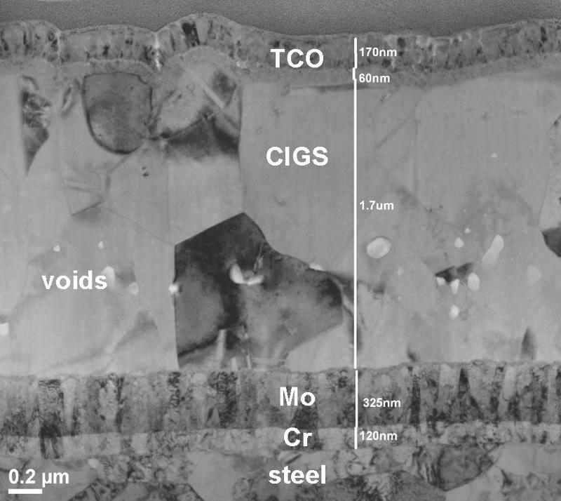
The Influence of Sputter Targets on the Manufacturing Costs and Efficiency of CIGS
|
From RenewableEnergyWorld.com, January 27, 2012: "The sputtering process is the most important technique for material deposition in CIGS-manufacturing. With innovative sputtering targets CIGS producers can significantly reduce their production costs. Manufacturers of sputtering targets like PLANSEE High Performance Materials have two approaches to reduce CIGS module manufacturing costs: In order to lower the material consumption by a better target utilization PLANSEE introduced the new monolithic and dogbone rotary target designs. With MoNa the company offers a new material alloy that increases conversion efficiencies."
Source: Read the full article...
RenewableEnergyWorld.com: http://www.renewableenergyworld.com/rea/partner/plansee-se/news/article/2012/01/the-influence-of-sputtering-targets-on-the-manufacturing-costs-and-efficiency-of-cigs
|
|
ORNL Finding has Materials Scientists Entering New Territory
|
From Oak Ridge National Laboratory, February 21, 2012: "Solar cells, light emitting diodes, displays and other electronic devices could get a bump in performance because of a discovery at the Department of Energy's Oak Ridge National Laboratory that establishes new boundaries for controlling band gaps.
 While complex transition metal oxides have for years held great promise for a variety of information and energy applications, the challenge has been to devise a method to reduce band gaps of those insulators without compromising the material's useful physical properties. While complex transition metal oxides have for years held great promise for a variety of information and energy applications, the challenge has been to devise a method to reduce band gaps of those insulators without compromising the material's useful physical properties.
The band gap is a major factor in determining electrical conductivity in a material and directly determines the upper wavelength limit of light absorption. Thus, achieving wide band gap tunability is highly desirable for developing opto-electronic devices and energy materials."
Source: Read the full article...
|
|
Hacking the SEM: Crystal Phase Detection for Nanoscale Sample
|
From NIST Material Measurement Laboratory, January 24, 2012:
"Custom modifications of equipment are an honored tradition of the research lab. In a recent paper, two materials scientists at the National Institute of Standards and Technology (NIST) describe how a relatively simple mod of a standard scanning electron microscope (SEM) enables a roughly 10-fold improvement in its ability to measure the crystal structure of nanoparticles and extremely thin films. By altering the sample 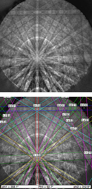 position, they are able to determine crystal structure of particles as small as 10 nanometers. The technique, they say, should be applicable to a wide range of work, from crime scene forensics to environmental monitoring to process control in nanomanufacturing. position, they are able to determine crystal structure of particles as small as 10 nanometers. The technique, they say, should be applicable to a wide range of work, from crime scene forensics to environmental monitoring to process control in nanomanufacturing.
The technique is a new way of doing electron diffraction with an SEM. In standard SEM-based electron diffraction, the researcher analyses patterns that are formed by electrons that bounce back after striking atoms in the sample. If the sample is a crystalline material, with a regular pattern to the arrangement of atoms, these diffracted electrons form a pattern of lines that reveals the particular crystal structure or 'phase' and orientation of the material."
Source: Read the full article...
|
|
Report on Health and Environmental Effects of Nanomaterials
|
From The National Academies, Office of News and Public Information, January 25, 2012: " Despite extensive investment in nanotechnology and increasing commercialization over the last decade, insufficient understanding remains about the environmental, health, and safety aspects of nanomaterials.Without a coordinated research plan to help guide efforts to manage and avoid potential risks, the future of safe and sustainable nanotechnology is uncertain, says a new report from the National Research Council.The report presents a strategic approach for developing research and a scientific infrastructure needed to address potential health and environmental risks of nanomaterials. Its effective implementation would require sufficient management and budgetary authority to direct research across federal agencies."
Source: Read the full article...
|
|
Sunlight Absorber: A Nanoscale Pattern Could Lead to More Efficient Solar Cells
|
From Technology Review, Published by MIT, March/April 2012, by TR Editors: "Thin films of silver ordinarily absorb only 5 percent of visible light. By applying a pattern of nanoscale shapes to such a surface, researchers increased absorption to 70 percent. The patterned film absorbs light from the entire visible spectrum and from almost any angle.
The advance could lead to solar cells that are far thinner and cheaper than conventional ones, because less semiconductor material would be needed to absorb sunlight. Researchers have known that nanoscale patterns can greatly enhance light absorption by gathering light waves the way antennas gather radio waves. But these patterns typically absorb only light of certain wavelengths, allowing most of the solar spectrum to escape. That makes them impractical for use in solar cells. The researchers have demonstrated that their patterns can be used to absorb a wide range of wavelengths, opening the door for their use in photovoltaic devices."
Source: Read the full article: "Broadband Polarization-Independent Resonant Light Absorption Using Ultrathin Plasmonic Superabsorbers", Harry Atwater et al., Nature Communications 2:517: http://www.technologyreview.com/energy/39660/
|
|
Researchers Develop New Methods to Fabricate Thin Films of Nanoparticles
|
From AZOnano.com, February 13, 2012, by Cameron Chai:
"Two techniques for fabricating gold monolayers, which are thin films of nanoparticles, have been devised by scientists at the Institute of Physical Chemistry of the Polish Academy (IPC PAS) in Warsaw. One technique is based on self-assembly, whereas the other utilizes the properties of salt solutions that are highly concentrated. Both these techniques assist in developing consistent, positively charged monolayers. Silicon and glass surfaces may produce a negative electric charge upon contact with water. The technique of depositing uniform and thin layers of gold nanoparticles, which are positively charged, on these surfaces appeared impossible until now. Instead of forming a consistent layer, the nanoparticles separated and created many clusters. Chemists generally include salt to the working solution to minimize the electrostatic interactions between the nanoparticles. The salt anions protected the nanoparticles, which is then able to deposit more tightly."
Source: Read the full article... AZOnano.com: http://www.azonano.com/news.aspx?newsID=24249 Image: AZOnano.com
|
|
DOE Plans New Energy Innovation Hub Focused on Advanced Batteries
|
From U.S. Department of Energy (DOE), February 7, 2012: "U.S. Secretary of Energy Steven Chu announced today plans to launch a new  Energy Innovation Hub for advanced research on batteries and energy storage with an investment of up to $120 million over five years. The hub, which will be funded at up to $20 million in fiscal year 2012, will focus on accelerating research and development of electrochemical energy storage for transportation and the electric grid. The interdisciplinary research and development through the new Energy Innovation Hub will help advance cutting-edge energy storage and battery technologies that can be used to improve the reliability and the efficiency of the electrical grid, to better integrate clean, renewable energy technologies as part of the electrical system, and for use in electric and hybrid vehicles that will reduce the nation's dependence on foreign oil."
Source: Read the full article...
|
|
Solar PV Equipment Replacements Expected to Ramp in Sales from 2013-2016
|
From ElectroIQ, February 14, 2012, by James Montgomery: "After a punishing 2011 and expectations of a tough 2012, there will be a surge of demand for upgrading solar photovoltaic (PV) manufacturing equipment over the next few years, says IMS Research.
PV equipment sales are expected to sink by more than half in 2012,  likely below the $6 billion range. (Some see tightness extending even into 2013.) But IMS has another take on the data: a v-shaped recovery that returns equipment spending to nearly 20% growth in both 2013 and 2014 and almost 40% in 2015. But with overcapacity still smothering new investments in production expansion, and with utilization rates at all-time lows, for now solar PV manufacturers will focus on upgrading and replacing aging equipment -- which IMS calculates as a $25 billion/20GW opportunity for equipment suppliers from now until 2016." likely below the $6 billion range. (Some see tightness extending even into 2013.) But IMS has another take on the data: a v-shaped recovery that returns equipment spending to nearly 20% growth in both 2013 and 2014 and almost 40% in 2015. But with overcapacity still smothering new investments in production expansion, and with utilization rates at all-time lows, for now solar PV manufacturers will focus on upgrading and replacing aging equipment -- which IMS calculates as a $25 billion/20GW opportunity for equipment suppliers from now until 2016."
Source: Read the full article...
|
|
Glass Industry Forecast: 2012 and Beyond
|
From Glass Magazine, January 24, 2012, Jenni Chase: "While overall construction levels will remain much the same this year, the spending  picture will be slightly different, analysts say, with commercial building and multifamily housing trending upward and institutional building continuing to fall. How will this affect the glass industry in the coming year? Industry leaders representing all segments of the market-from float glass manufacturers, to fabricators, to glaziers, retailers, and suppliers- share their perspective in the individual stories..."
Source: Read the full article...
Glass Magazine: http://glassmagazine.com/www.glassmagazine.com/2012forecast
|
|
New Form of Hafnium Oxide Boosts Dielectric Constant from 20 over 30
|
From Semiconductor Today, February 2012: "A novel material developed by researchers at the University of Cambridge is opening up new possibilities for next-generation electronic and optoelectronic devices, and paving the way for further component miniaturization. Developed by Dr Andrew Flewitt's research team in the Department of Engineering's Electronic Devices & Materials Group, the new form of hafnium oxide provides higher dielectric constant compared with existing forms of hafnium oxide, which is already a key material in the electronics industry. Normally, metal oxides are produced on substrates by sputtering (where some of the atoms of an electrode are ejected as a result of bombardment by heavy positive ions). However, one of the problems when attempting to make high-quality electronic materials through sputtering is the difficulty in precisely controlling the energetics of the deposition process, and hence the material properties such as defect density."
Source: Read the full article... Semiconductor Today: http://www.semiconductor-today.com/news_items/2012/FEB/CAMBRIDGE_070212.html
|
|
Bilayer Graphene Works as an Insulator
|
From University of California Riverside (UCR) Newsroom, January 24, 2012: "A research team led by physicists at the University of California, Riverside has identified a property of "bilayer graphene" (BLG) that the researchers say is analogous to finding the Higgs boson in particle physics.
Graphene, nature's thinnest elastic material, is a one-atom thick sheet of carbon atoms arranged in a hexagonal lattice. Because of graphene's planar and chicken wire-like structure, sheets of it lend themselves well to stacking. carbon atoms arranged in a hexagonal lattice. Because of graphene's planar and chicken wire-like structure, sheets of it lend themselves well to stacking.
BLG is formed when two graphene sheets are stacked in a special manner. Like graphene, BLG has high current-carrying capacity, also known as high electron conductivity. The high current-carrying capacity results from the extremely high velocities that electrons can acquire in a graphene sheet.
The physicists report online Jan. 22 in Nature Nanotechnology that in investigating BLG's properties they found that when the number of electrons on the BLG sheet is close to 0, the material becomes insulating (that is, it resists flow of electrical current) - a finding that has implications for the use of graphene as an electronic material in the semiconductor and electronics industries."
Source: Read the entire article... UCR Newsroom: http://newsroom.ucr.edu/2843 Image: Lau lab, UC Riverside
|
|
Flexible Terahertz Metamaterial is Useful in Stealth Applications
|
From Laser Focus World, January 11, 2012, by John Wallace: "A flexible metamaterial film created by researchers at the Technical University of Denmark (Lyngby, Denmark) and Boston University (Boston, MA) drastically reduces reflection of terahertz radiation, and can serve as a "stealth" material to minimize objects' radar cross-section at terahertz frequencies. The material was wrapped around a metallic cylinder for test, reducing the cylinder's cross-section by close to 400 times at 0.87 THz.
The film consists of a 12-μm-thick polyimide (PI) layer, a 200-nm-thick layer of gold (Au), a second 12-μm-thick layer of PI, and a second 200-nm-thick layer of Au patterned by photolithography."
Source: Read the entire article...
|
|
New Nano-Material Combinations Produce Leap in Infrared Technology
|
From Arizona State University (ASU) News, Science & Tech, February 13, 2012:
"Arizona State University researchers are finding ways to improve infrared photodetector technology that is critical to national defense and security systems, as well as used increasingly in medical diagnostics, commercial applications and consumer products. A significant advance is reported in a recent article in the journal Applied Physics Letters. It details discovery of how infrared photodetection can be done more effectively by using certain materials arranged in specific patterns in atomic-scale structures. It's being accomplished by using multiple ultrathin layers of the materials that are only several nanometers thick. Crystals are formed in each layer. These layered structu res are then combined to form what are termed 'superlattices.' res are then combined to form what are termed 'superlattices.' The unique property of the superlattices is that their detection wavelengths can be broadly tuned by changing the design and composition of the layered structures. The precise arrangements of the nanoscale materials in superlattice structures helps to enhance the sensitivity of infrared detectors, Zhang says."
Source: Read the entire article...
|
|
26 Tutorial Courses at the SVC TechCon in Santa Clara
|
Anyone can take advantage of the practical, problem-solving tutorial courses offered by SVC. Taught by some of the most respected professionals in the vacuum coating industry, these tutorial courses cover every aspect of vacuum coating and complement the technical conference sessions and exhibit. Twenty-six tutorial courses will be offered, including six new topics. The Education Program takes place from April 28 - May 3, 2012 during the SVC TechCon in Santa Clara, California at the Santa Clara Convention Center.
DISCOUNTS: Discounted fees are available for full-time students. Discounts are offered to multiple registrations from one organization. A 25% discount is given on each tutorial  registration for the second or more employee in a company who enroll in the same tutorial. (Does not apply to student rate.) registration for the second or more employee in a company who enroll in the same tutorial. (Does not apply to student rate.)
The TechCon Tutorial Course Roster, course description, topical outline, detailed syllabus, instructor biographical sketch, and tutorial course fees are available at www.svc.org.
Register for Tutorial Courses via the 2012 TechCon Registration page.
|
|
Do You Have an Interesting Article to Share?
|
Interested in sharing the latest news in vacuum coating technology? Forward us a link to an article you want to share with the rest of the SVC readership to publications@svc.org. Purchase advertising space in this newsletter by contacting SVC at  svcinfo@svc.org. svcinfo@svc.org.
Society of Vacuum Coaters
71 Pinon Hill Place NE
Albuquerque, New Mexico 87122
505-856-7188
|
|
|
|
|