INFICON thin film deposition controllers, monitors and accessories, including customizable sensors and feedthroughs, offer features, function and value targeted to your application. View our catalog and contact us today! |
Reliable, Low Cost Rotary Motion Feedthroughs
Rigaku solid-shaft Superseal rotary motion feedthroughs are the ultimate value, rotary sealing solution. They are the lowest cost feedthroughs while being recognized for their quality and performance. Learn More.
Rigaku Vacuum Products
E-mail: vacuum-info@rigaku.com
Phone: 603-890-6001
|
Got a Handle on Destructive Arching? Comdel Can Help.
Comdel's VF Series Multiple Channel Synthesizers provide phase adjustable output to avoid destructive arcing and cross-talk in multiple cathode plasma processing chambers, and allows adjustment for cable length dependencies. Learn more.
Comdel
11 Kondelin Road
Gloucester, MA 01930
Tel: 978-282-0620 or 800-468-3144
Fax: 978-282-4980
www.comdel.com
info@comdel.com
|

MDC's Bundled Engineered Solutions
MDC offers virtually every component required for vacuum coating applications. With MDC's standard chamber line you have the advantage of bundling these high quality pieces together without hours or weeks of special engineering. More...
MDC
engineered process solutions
www.mdcvacuum.com
|
|
From AR Coatings to Notch Filters, and from TCOs to DBRs, Evatec offers customized coating platforms and complete process solutions based on enhanced evaporation and sputter.
Phone: (603) 669-9656
www.evatecnet.com
E-Mail:infoNA@evatecnet.com
|
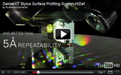
Measure Thin Film Deposition
with DektakXTTM
Bruker's new DektakXTTM stylus profiler monitors thin film deposition and etch systems with the industry's best measurement repeatability (<5Å). Find out how to better control your thin film process development faster, easier and more accurately. Learn More.
Bruker Corporation
520-741-1044
productinfo@bruker-nano.com
|

Rotary Vane Pumps
Stock to 4 Weeks
3 to 64 CFM, 6 to108 m3/hour. All voltages, 1 and 3 phase. Fomblin/Krytox available. 2 year parts and labor warranty, satisfaction guaranteed.
Vacuum Research Corporation Phone: 800/426-9340
Web: www.vacuumresearch.com
E-Mail: vrc@vacuumresearch.com
|
Dynavac produces a wide range of thin film deposition systems that include electron beam, thermal evaporation, sputtering and ion-assist. Our reputation is built upon quality, reliability, and excellent customer relations.
Telephone: 781-740-8600 |
|
New Print Catalog Available from
UC Components Inc.
www.uccomponents.com
|
Evans Analytical Group (EAG) is the leading global provider of high quality surface analysis and materials characterization services to the films and coatings industry.
Evans Analytical Group
1.800.366.3867
|

Solid Sealing Technology designs and manufactures hermetic assemblies using metalizing, brazing and glass-ceramic sealing including standard and custom Feedthroughs/Connectors for extreme environments and UHV.
Contact:
Ph: 518-874-3600
Fax: 518-874-3610
info@solidsealing.com
|
Thin-Films Research is prepared to meet your custom thin-film coating requirements. Using state-of-the-art equipment and over 40 years of experience, Thin-Films Research offers technology for the electro-optics, semiconductors, sensors & medical electronic industries. Learn More
Thin-Films Research, Inc.
270 Littleton Road
Westford, MA 01886
Phone: 978-692-9530
Fax: 978-692-9531
E-Mail: sales@thinfilmsresearch.com |
Custom Cubical Vacuum Chambers
Pfeiffer Vacuum offers two week lead time and pricing starting at $5900 for 12" and $7400 for 20" custom cubical vacuum chambers. Other chamber sizes and shapes are also available.
Pfeiffer Vacuum, Inc.
24 Trafalgar Square
Nashua, NH 03063-1988
Phone: 603-578-6500
Web site: www.trinos.com
hardware@pfeiffer-vacuum.com
|
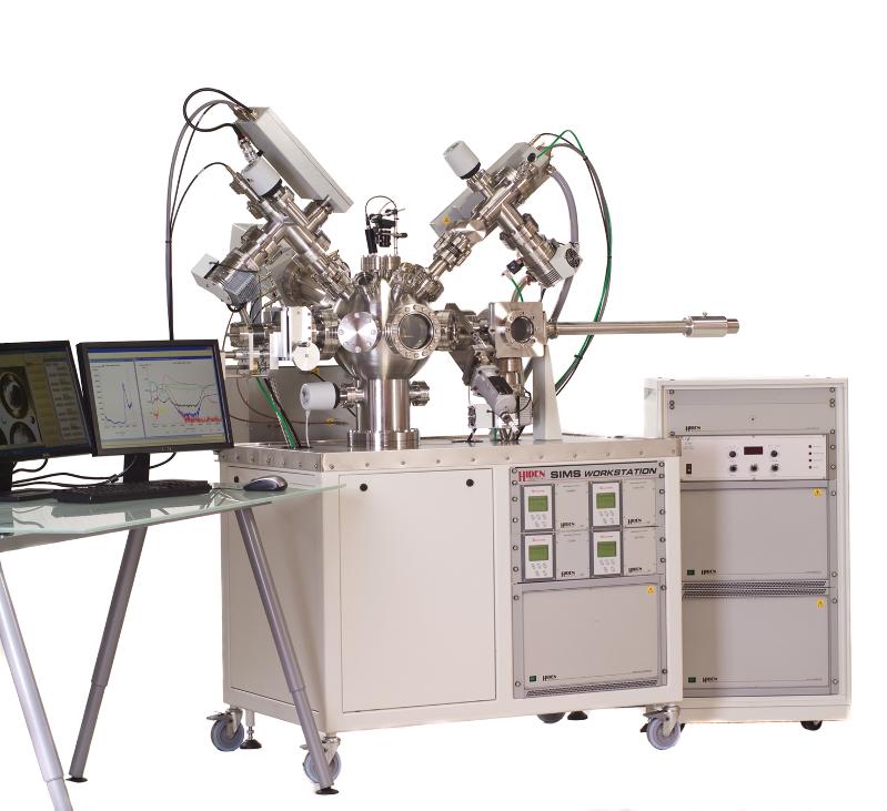
SIMS Workstation
A high performance SIMS instrument for:
- Thin film depth profiling
- Surface imaging
- Features new high sensitivity sputtered neutrals detection mode for quantitative analysis.
Learn more.
E-mail address: info@hiden.co.uk
Phone: +44 [0] 1925 445225 (UK)
or [1] 734 542 6666 (USA)
Website: www.HidenAnalytical.com
|
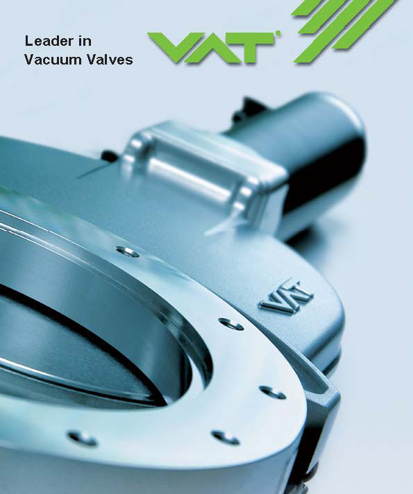
VAT manufactures high quality vacuum valves for a variety of applications. Products include: gate, angle, fast-closing, transfer, pendulum, throttle, pressure control, all-metal and customized valves. Learn more.
Contact Us:
Phone: 781-935-1446
or 800-935-1446
E-Mail: US@vatvalve.com
|
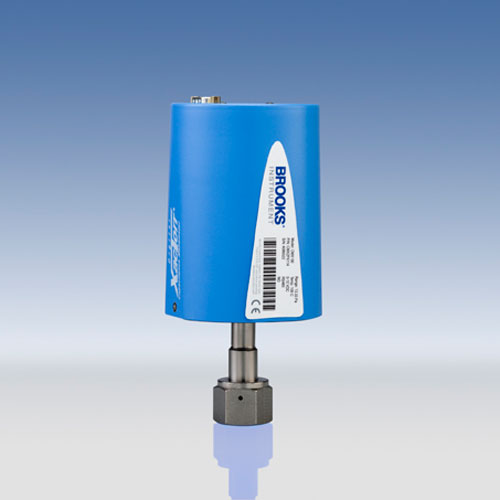
Capacitance Manometers that Last
...Up to 3x Longer
The rugged design of the Brooks XacTorr handles byproduct build-up, lasting up to three times longer even in aggressive processes. Learn more.
Brooks Instrument
Phone: 215.362.3700
Email:
BrooksAM@BrooksInstrument.com
|

Gas Analysis - Low Cost RGA
ULVAC offers three compact quadrupole mass spectrometers - the low cost Qulee BGM, Qulee CGM for high pressures and Qulee HGM for the highest sensitivity. Learn More.
|

April 28 - May 3, 2012
Santa Clara, California
Technical Program
Exhibit
Education
Networking
Learn More...
|
UPCOMING LIVE WEBINARS
Sputter Deposition
David Glocker, Isoflux Incorporated
Wednesday, February 29, 2012
11:00 a.m. - 2:00 p.m. EST
Basics of Vacuum Web CoatingDonald J. McClure, Acuity ConsultingThursday, June 7, 201211:00 a.m. - 2:00 p.m. EDTON-DEMAND WEBINAR
Practical Aspects of Plasma Modification of Polymer Materials and Plasma Web TreatmentJeremy Grace, Eastman Kodak |
|
|

|
|
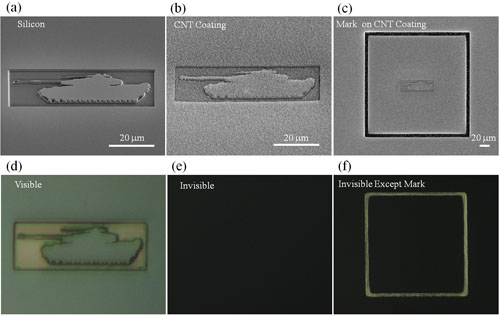
Perfect Black Coating Can Render a 3D Object Flat
|
From University of Michigan News Service, November 22, 2011, by Nicole Casal Moore: "A carbon nanotube coating developed at the University of Michigan acts as a 'magic black cloth' that conceals an object's three-dimensional geometry and makes it look like a flat black sheet. The 70-micron coating, or carbon nanotube carpet, is about half the thickness of a sheet of paper. It absorbs 99.9 percent of the light that hits it, researchers say.
'You could use it to completely hide any 3D attributes of an object,' said Jay Guo, a professor in the Department of Electrical Engineering and Computer Science and principal investigator.
'It's not cloaking, as the object can still cast a shadow. But if you put an object on a black background, then with this coating, it could really become invisible.'
A paper on the research is newly published online in Applied Physics Letters."
Source: Read the full article...
University of Michigan News Service: http://ns.umich.edu/new/releases/20088-perfect-black-coating-can-render-a-3d-object-flat-raises-intriguing-dark-veil-possibility-in-astronomy
Image: University of Michigan News Service
|
|
Has Thin Film Weathered the 'Perfect Storm'
|
From PV Insider, November 28, 2011, by Matt Carr: "The year 2011 will be remembered as a turbulent year for the thin film industry, and the US market in particular has had its fair share of well publicized difficulties. The collapse of Solyndra provided the stick whic h thin film's critics used to beat the technology, particularly as the company was held up as a bastion for US jobs in renewables. h thin film's critics used to beat the technology, particularly as the company was held up as a bastion for US jobs in renewables.
The recent announcement that Michigan-based Energy Conversion Devices have placed an indefinite suspension on their manufacturing puts the spotlight back on to the technology. But is thin film really on the brink? Or can a leaner, fitter thin film industry bounce back stronger?
Thin film PV has a role to play in the solar market, and it is inevitable that any emerging technology market will go through rounds of spectacular growth and heartbreaking consolidation. It is vital now to establish what is fact and what is fiction about thin film and its PV competitors, and not to overstate the failures or glorify the successes."
Source: Read the full article...
PV Insider: http://news.pv-insider.com/thin-film-pv/has-thin-film-weathered-%E2%80%98perfect-storm%E2%80%99
Image: PV Insider
|
|
Slippery When Stacked: NIST Theorists Quantify the Friction of Graphene
|
From NIST Tech Beat, January 10, 2012,: "Similar to the way pavement, softened by a hot sun, will slow down a car, graphene-a one-atom-thick sheet of carbon with wondrous properties-slows down an object sliding across its surface. But stack the sheets and graphene gets more slippery, say theorists at the National Institute of Standards and Technology (NIST), who developed new software to quantify the material's friction.
"I don't think anyone expects graphene to behave like a surface of a three-dimensional material, but our simulation for the first time explains the differences at an atomic scale," says NIST postdoctoral researcher Alex Smolyanitsky, who wrote the modeling program and co-authored a new paper about the study. "If people want to use graphene as a solid-state lubricant or even as a part of flexible electrodes, this is important work." 
Their research paper: A. Smolyanitsky, J.P. Killgore and V.K. Tewary, 'Effect of elastic deformation on frictional properties of few-layer graphene' is published in Physical Review B.
Source: Read the full article...
|
|
Almost Perfect: Michigan Tech Researcher Nears Creation of Superlens
|
From Michigan Tech News, January 16, 2012, by Marcia Goodrich:
"A superlens would let you see a virus in a drop of blood and open the door to better and cheaper electronics. It might, says Durdu Guney, make ultra-high-resolution microscopes as commonplace as cameras in our cell phones.
No one has yet made a superlens, also known as a perfect lens, though people are trying. Optical lenses are limited by the nature of light, the so-called diffraction limit, so even the best won't usually let us see objects smaller than 200 nanometers across, about the size of the smallest bacterium. Scanning electron microscopes can capture objects that are much smaller, about a nanometer wide, but they are expensive, heavy, and, at the size of a large desk, not very portable.
Now Prof. Guney, an assistant professor of electrical and computer engineering at Michigan Technological University, has taken a major step toward creating superlens that could use visible light to see objects as small as 100 nanometers across.
Source: Read the full article...
|
|
ALD to Enable Novel, High Efficiency Silicon Nanorod Solar Cells
|
From Picosun Oy (Epsoo, Finland), December 31, 2011: "Picosun Oy, Finland-based global manufacturer of state-of-the-art Atomic Layer Deposition (ALD) equipment, reports successful final results of the European Union 7th Framework Programme funded research project ROD-SOL. The goal of this multinational, inter-European, three years (2009-2011) project combining the efforts of both scientific and industrial partners has been to dramatically increase the efficiency of solar cells and reduce the costs of their manufacturing. This has been achieved with novel, innov  ative, silicon nanorod based concept. The amount of active photovoltaic material (Si) can be significantly reduced by growing the light-trapping nanorod "forests" (thickness from < 1μm to a few μm at most) on cheaper substrates such as glass or flexible foils. This has led to already promising over 9% energy conversion efficiencies with very good long-term stabilities of cells."
Source: Read the full article...
|
|
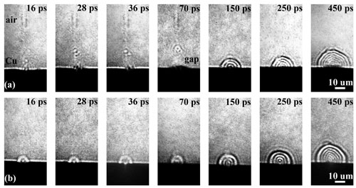
Research Could Improve Laser-Manufacturing Technique
|
From Purdue University News Service, December 19, 2011, by Emil Venere: "Engineers have discovered details about the behavior of ultrafast laser pulses that may lead to new applications in manufacturing, diagnostics and other research. Ultrafast laser pulses are used to create features and surface textures in metals, ceramics and other materials for applications including the manufacture of solar cells and biosensors. The lasers pulse at durations of 100 femtoseconds, or quadrillionths of a second, and cause electrons to reach temperatures greater than 60,000 degrees Celsius during the pulse duration. The pulses create precise patterns in a process called 'cold ablation,' which turns material into a plasma of charged particles."
Source: Read the full article... Purdue University: http://www.purdue.edu/newsroom/research/2011/111219ShinPlasma.html Image: Yung Shin, Purdue University School of Mechanical Engineering
|
|
Record-Breaking Thin Films Use Nano-Dielectric
|
From ElectronicsWeekly.com, January 4, 2012, bu Steve Bush:
"The world's highest performance thin-film capacitors are being claimed by researchers at the International Center for Materials Nanoarchitectonics (MANA) near Tokyo. Key is a high-permittivity (high-k) dielectric sheet around 1nm thick. Dr Minoru Osada and colleagues created thin films based on titanium-niobate (TiNbO5, Ti2NbO7, Ti5NbO14) nano-sheets by delaminated layered oxides and stacking the sheets on an atomically flat SrRuO3 substrate, creating films 5-15nm thick.
'The solution-based room-temperature process using oxide nano-sheets as building blocks opens multiple possibilities for the development of high-k dielectrics in capacitor technology, gate insulators in organic field effect transistors, energy-storage devices, and also future flexible electronics,' said the Center. Thin-film capacitors made with these films achieve a permittivity of 160-300."
Source: Read the full article... ElectronicsWeekly.com: http://www.electronicsweekly.com/Articles/04/01/2012/52636/record-beaking-thin-films-use-nano-dielectric.htm
|
|
Volatility of Rare Earth Market Challenges Manufacturers
|
From SPIE Newsroom, January 9, 2012, by Ford Burkhart: "Self-sufficiency in critical rare-earth supplies is the goal of photonics and optics leaders after the 2011 rollercoaster ride of pricing combined with fear of cutoffs or cutbacks in availability. Products dependent on REEs (rare earth elements) include wind 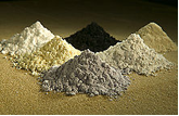 turbines, batteries for hybrid vehicles, lasers and optical fibers, polishing compounds for lenses, and many other military and clean-energy applications. The price of many REE products multiplied to five or six times the 2010 levels after China announced export restrictions on the 17 REEs -- in particular cerium oxide, used in polishing high-precision optics. As of now, China seems not to want to set new quotas or halt the export of REEs but is expected to limit exports to current levels."
The optics industry is using several strategies to make sure future needs are met: - Redesign of products and processes
- Moving toward recycling
- Stockpiling
- Exploration for new sites
- Lobbying policymakers
Source: Read the full article...
|
|
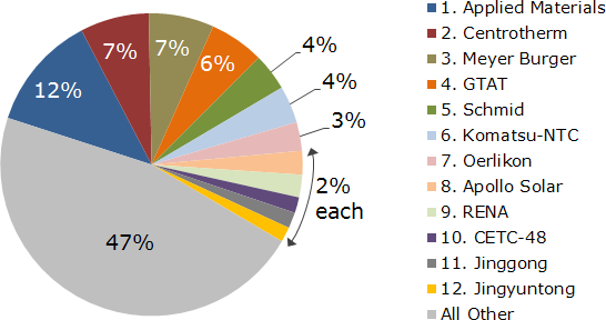
Chinese PV Equipment Suppliers Grab Further Market-Share Gains
|
From NPD Display Search, PV Equipment Quarterly, January 16, 2012: ""Ambitious PV manufacturing capacity investments across the Asia Pacific region during 2011 have provided substantial revenue growth for local PV equipment suppliers, according to the latest NPD Solarbuzz PV Equipment Quarterly report. Beneficiaries of these record investments include Japanese wire-saw producer Komatsu-NTC and an emerging group of Chinese tool suppliers. Collectively, these four Chinese companies have posted a CAGR metric in excess of 200% for PV-specific equipment revenues covering the period from 2008 to 2011. Applied Materials is forecast to retain the top spot as leading PV equipment supplier by recognized revenues."
Source: Read the full article...
|
|
Gallium Nitride (GaN) Gaining Traction in Commercial Applications
|
From Strategy Analytics, January 4, 2012: "Despite continuing dominance by military applications, gallium nitride (GaN) technology is also seeing widespread deployment in commercial applications. The " GaN Microelectronics Market Update 2010-2015" report, recently released by Strategy Analytics to its GaAs and Compound Semiconductor Technologies Service (GaAs) and its Advanced Defense Systems Service (ADS) subscribers, forecasts that the overall GaN device market will grow at a CAAGR of nearly 29 percent, to reach $178 million in 2015. During this time, commercial applications, led by CATV and high power electronics will grow from less than one million dollars to reach nearly $58 million.
This Strategy Analytics report predicts that military applications will continue to lead the way, but the percentage of the total GaN revenue derived from military applications will shrink from 98 percent in 2010 to 67percent in 2015. In addition, Strategy Analytics forecasts that revenue growth rates for GaN devices in wireless infrastructure, high power electronics and CATV/VSAT (very small aperture terminals) will all exceed 100 percent."
Source: Read the full article...
Strategy Analytics: http://www.strategyanalytics.com/default.aspx?mod=pressreleaseviewer&a0=5155
|
|
NREL Scientist Report First Solar Cell Producing More Electrons in Photocurrent than Solar Photons Entering Cell
|
From National Renewable Energy Laboratory (NREL), December 15, 2011: "Researchers from the U.S. Department of Energy's National Renewable Energy Laboratory (NREL) have reported the first solar cell that produces a photocurrent that has an external quantum efficiency greater than 100 percent when photoexcited with photons from the high energy region of the solar spectrum.
The external quantum efficiency for photocurrent, usually expressed as a percentage, is the number of electrons flowing per second in the external circuit of a solar cell divided by the number of photons per second of a specific energy (or wavelength) that enter the solar cell. None of the solar cells to date exhibit external photocurrent quantum efficiencies above 100 percent at any wavelength in the solar spectrum.
The external quantum efficiency reached a peak value of 114 percent. The newly reported work marks a promising step toward developing Next Generation Solar Cells for both solar electricity and solar fuels that will be competitive with, or perhaps less costly than, energy from fossil or nuclear fuels."
Source: Read the full article... NREL Newsroom: http://www.photonics.com/Article.aspx?AID=48531
|
|
Striped Nano-Cavity Arrays Created in PEDOT-PSS Thin Films
|
From Nanotechweb.org, Jan 6, 2012, by Dajun Yuan et al.: "The strong near-field optical enhancement of pulsed laser radiation using self-assembled nanospheres as an array of lenses offers a route to massively parallel nanoscale surface patterning, while laser interference lithography opens the door to periodic patterning with tunable periodicity over large areas. In recent work published in the journal.
Nanotechnology, researchers from Georgia Tech, Fraunhofer IWS, Biotectix LLC and the University of Delaware have combined these two techniques to create periodic stripes of nano-cavity arrays in thin films of PEDOT-PSS.
The team built a laser 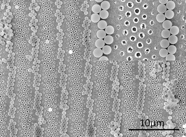 interference patterning system for a frequency-tripled, nanosecond pulsed Nd:YAG laser emitting 355 nm wavelength light. First, hexagonally closed-packed monolayers of silica nanospheres were obtained on the PEDOT-PSS thin films through self-assembly using spin coating. Then, single laser beam and dual-beam interference patterns were irradiated onto the self-assembled monolayers." interference patterning system for a frequency-tripled, nanosecond pulsed Nd:YAG laser emitting 355 nm wavelength light. First, hexagonally closed-packed monolayers of silica nanospheres were obtained on the PEDOT-PSS thin films through self-assembly using spin coating. Then, single laser beam and dual-beam interference patterns were irradiated onto the self-assembled monolayers."
Source: Read the summary of the paper. The full paper is found in the Journal "Nanotechnology"... Nanotechweb.org: http://nanotechweb.org/cws/article/lab/48243 Image: Nanotechweb.org
|
|
Correction...
|
In the January issue of SVConnections, we featured an article erroneously listing Chalmers University of Technology as residing in the United Kingdom. Chalmers University of Technology is located in Gothenburg, Sweden. We regret the error and apologize for any confusion.
|
|
Do You Have an Interesting Article to Share?
|
Interested in sharing the latest news in vacuum coating technology? Forward us a link to an article you want to share with the rest of the SVC readership to publications@svc.org. Purchase advertising space in this newsletter by contacting SVC at  svcinfo@svc.org. svcinfo@svc.org.
Society of Vacuum Coaters
71 Pinon Hill Place NE
Albuquerque, New Mexico 87122
505-856-7188
|
|
|
|
|