|
|
|
|
   Society of Vacuum Coaters Society of Vacuum Coaters | May 2014 |
|
|
|
|
|
|
|
|
|
|
 
Opportunities for Functional Design Using PVD and UV-Curable Coatings
From RadTech Report, Issue 1 2014 (March), by Jason T. Eich, Eileen Weber, Phil Abell, Kristy Wagner and Chris Mack
"Interest in alternatives to electroplated chrome is expanding dramatically. Color and appearance effects are limited with traditional chrome electroplating and successful "paint-on-chrome" applications are expensive and highly proprietary. Collectively, the automotive, home appliance and cosmetic markets are actively searching for alternatives with the appearance and durability of electroplating, but without the environmental side effects; appearance and functional design limitations; and costs associated with this decades-old process."
|
 Tiny Step Edges, Big Step for Surface Science Tiny Step Edges, Big Step for Surface Science
From Vienna University of Technology, April 9, 2014,
by Florian Aigner
"Experiments at the Vienna University of Technology can explain the behavior of electrons at tiny step edges on titanium oxide surfaces. This is important for solar cell technology and more effective catalysts.
Professor Ulrike Diebold and her team at the Vienna University of Technology managed to find out why oxygen atoms attach so well to tiny step edges at titanium oxide surfaces. Electrons accumulate precisely at these edges, allowing the oxygen atoms to connect more strongly. In solar cells, this effect should be avoided, but for catalysts this can be highly desirable."
|
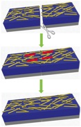 Self-healing Carbon Nanotube Supercapacitors Self-healing Carbon Nanotube Supercapacitors
From Nanowerk Spotlight, March 10, 2014
by Michael Berger
"A team led by Xiaodong Chen, an associate professor in the School of Materials Science & Engineering at Nanyang Technological University,
has designed and fabricated the first integrated, mechanically and electrically self-healing supercapacitor by spreading functionalized
single-walled carbon nanotube (SWCNT) films
on self-healing substrates."
|
 Bendable Silicon Electronics Bendable Silicon Electronics
From Chemical and Engineering News, February 24, 2014
"By shaving off an ultrathin layer from the top of a silicon wafer, researchers can transform rigid electronic devices into flexible ones. It's developers say the new method is more cost-effective than similar techniques. The group's new process uses standard techniques and works with monocrystalline silicon, a relatively inexpensive and common form of silicon.
After fabricating devices on a wafer, the researchers deposit a thin silicon dioxide film over the entire surface. Using photolithography and reactive ion etching, the team next bores 5-µm-wide pores in the oxide film and the underlying silicon. They then expose the wafer to xenon difluoride gas. It passes through the pores and etches away a layer of silicon micrometers below the wafer's surface to release the ultrathin top layer carrying the devices."
|
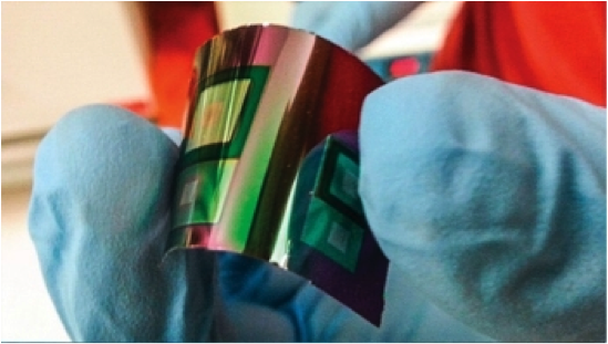
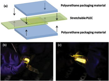 Intrinsically Elastomeric Polymer Light-Emitting Devices Intrinsically Elastomeric Polymer Light-Emitting Devices
From Information Display, January/February 2014, by Jiajie Liang and Qibing Pei
"Stretchable or ultra-flexible electronics and optoelectronics have emerged as alternative technologies for the next generation of electronic applications. These elastomeric light-emitting display and solid-state lighting systems are fabricated on substrates that can be stretched, twisted, and folded - they are often referred to as skin-like displays. True stretchability is much more demanding than flexibility.
ITO has been the ubiquitous transparent conductive electrode material for practically all forms of displays. However, ITO routinely cracks under an applied strain of ~1%."
Image: Information Display
|
 Tesla's Gigafactory and Tesla's Gigafactory and
Energy Storage Aims
From Renewable Energy World, March 03, 2014,
by James Montgomery
"Tesla made a splash with its proposed $5 billion "Gigafactory" and its eye-popping numbers: a 10 million square foot facility on an entire land area of 500-1,000 acres, with output of 35 GWh/year of battery cells and 50 GWh/year of battery packs by 2020. That'll be enough to support 500,000 of the company's forthcoming Gen-3 vehicles, compared with a little over 20,000 annual demand for its cars today. By comparison, the entire lithium-ion battery supply-chain produced about 34 GWh in 2013, the vast amount going not to electric vehicles but consumer electronics."
Image: Tesla
|
 Two New Public-Private Manufacturing Innovation Institutes Named Two New Public-Private Manufacturing Innovation Institutes Named
From The White House,
Office of the Press Secretary, February 25, 2014
"President Obama announced "two new manufacturing innovation institutes led by the Department of Defense supported by a $140 million Federal commitment combined with more than $140 million in non-federal resources: (1) Detroit-area headquartered consortium of businesses and universities" led by EWI "with a focus on lightweight and modern metals manufacturing" for defense, aerospace, automotive, energy, and consumer products industries; (2) "Chicago headquartered consortium of businesses and universities" led by UI Labs "that will concentrate on digital manufacturing and design technologies."
Image: The White House |
 Monolayer Tungsten Diselenide Shows Promise Monolayer Tungsten Diselenide Shows Promise
for Optoelectronics
From MIT News, March 10, 2014,
by David Chandler
"A team of MIT researchers has used a novel material that's just a few atoms thick to create devices that can harness or emit light. This proof-of-concept could lead to ultrathin, lightweight, and flexible PV cells, LEDs, and other optoelectronic devices.
The material they used, called tungsten diselenide (WSe2), is part of a class of single-molecule-thick materials under investigation for possible use in new optoelectronic. In these experiments, the MIT researchers were able to use the material to produce diodes, the basic building block of modern electronics."
Image: MIT/ Britt Baugher and Hugh Churchill |
 Semiconductor Fab Equipment Spending to Increase 20-30% in 2014 Semiconductor Fab Equipment Spending to Increase 20-30% in 2014
From SEMI, March 5, 2014
"The SEMI World Fab Forecast update reveals a 20 to 30 percent projected increase in semiconductor fab equipment spending in 2014. The uptick to 30 percent depends on specific fab projects in the Europe/Mideast and Asia regions. The report identified over 190 fab projects in 2014 spending on construction and/or equipment and over 250 projects in 2015."
Source: SEMI, http://www.semi.org
Image: SEMI |
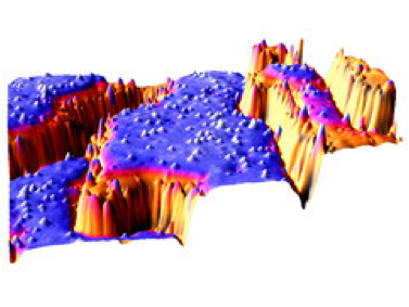
 Patterning of Surface Changes Coercivity of Material by as Much Patterning of Surface Changes Coercivity of Material by as Much
as 80 Percent
From North Carolina State University, March 17, 2014,
by Matt Shipman
"Researchers from North Carolina State University have found a way to reduce the coercivity of nickel ferrite (NFO) thin films by as much as 80 percent by patterning the surface of the material, opening the door to more energy efficient high-frequency electronics, such as sensors, microwave devices and antennas.
Coercivity is a property of magnetized materials and is the amount of magnetic field needed to bring a material's magnetization to zero. Basically, it's how much a material likes being magnetic. For devices that rely on switching current back and forth repeatedly - such as most consumer electronics - you want materials that have low coercivity, which improve device performance and use less energy."
Source: North Carolina State University, http://news.ncsu.edu
Image: North Carolina State University/Goran Rasic
|
 Metal Mesh Competitive Metal Mesh Competitive
as Transparent Conductor
for Large Panels
From Nanomarkets, April 2, 2014
"Metal meshes - previously not under serious consideration as transparent conductors because of their lack of transparency - have now overcome their performance limitations and are seen as serious competition for ITO in several applications, especially those that require large panels for displays, lighting, or solar energy. Metal meshes can therefore provide a performance advantage, creating panels with more uniform and greater brightness.
Bringing metal meshes into larger displays can be a way for metal mesh manufacturers to increase their revenue streams. One challenge is to demonstrate performance in high volume production of large panels. Another is that manufacturers say they are cost-competitive with ITO, but they will need to be priced lower than ITO to really be competitive."
Image: Wikipedia (Times Square) |
 Stretchable Energy Storage and Conversion Stretchable Energy Storage and Conversion
From Nanowerk Spotlight, March 20, 2014, by Michael Berger
"Stretchable electronics are mechanically robust electronics which can be bent, folded, crumpled and stretched and are a major research focus of nanotechnology scientists towards next-generation wearable and implantable devices.
Stretchable energy storage and conversion devices are key components for the fabrication of complete and independent stretchable systems. In a recent review in Small ("Stretchable Energy Storage and Conversion Devices"), researchers summarize the recent progresses in the developments of stretchable power sources including supercapacitors, batteries and solar cells. They discuss representative structural and material designs to impart stretchability to the originally rigid devices and analyze advantages and drawbacks associated with the various fabrication methods. They also present summaries of the research progresses along with future development directions."
Image: Nanowerk Spotlight/ AAAS |
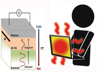 Spintronic Thermoelectric Power Generators Spintronic Thermoelectric Power Generators
From The University of Utah, March 21, 2014
"Imagine a computer so efficient that it can recycle its own waste heat to produce electricity. While such an idea may seem far-fetched today, significant progress has already been made to realize these devices. Researchers at the Nanostructured Materials Research Laboratory at the University of Utah have fabricated spintronics-based Bi doped YIG thin film devices which do just that, i.e. convert even minute waste heat into useful electricity. Spintronics is a new branch of electronics which utilizes both the charge as well as the spin of electrons.
Their spintronic-based thermoelectric devices work at room temperature and don't require the continuous application of an external magnetic field. Most of the spintronic thermoelectric devices in earlier studies required the continuous application of a magnetic field to keep the device magnetized."
Image: University of Utah/ Gene Siegel and Shiang Teng |
 Growth Method for Chalcongenide Phase-Change Nanostructures Growth Method for Chalcongenide Phase-Change Nanostructures
From NASA Tech Briefs, Ames Research Center, Moffett Field, CA April 2014
"Phase-change materials (PCMs) are among the most promising media for nonvolatile, re-writable, and highly durable data storage applications. Phase change materials based on the Ge-Sb-Te (GST) multi-element alloy system and other materials have been extensively studied and have been found to be suitable for optical and electrical memories. Resistive switching PRAM (phase change random access memory) devices, using a thin film form of these materials, have been shown to provide faster write/read, improved endurance, and simpler fabrication as compared with the transistor-based nonvolatile memories."
Image: NASA Ames Research Center |
 Multicolored Crystals Synthesized for Bar Codes Multicolored Crystals Synthesized for Bar Codes
From Chemical and Engineering News, March 31, 2014, by JK
"Luminescent materials find wide use in areas such as anticounterfeiting and biological sensors, especially when patterned as bar codes. Such materials, however, can be difficult to make or required expensive instrumentation to detect. New microrods can be easily synthesized to emit multiple colors by doing with various lanthanides, reports a group at the National University of Singapore. The rods are composed of NaYF4 and doped with ytterbium, thulium, or erbium in varying proportions to emit blue, green or red light in response to infrared radiation."
Image: Chemical and Engineering News |
|
|
|
|
|
Upcoming Events
|
 |
7th Symposium on Functional Coatings and Surface Engineering
(FCSE-2014)
Montreal, Quebec, Canada
The symposium will feature the latest advances in the area of deposition and surface engineering processes, materials and properties of coatings and thin film systems suitable for optical, optoelectronic, aerospace, energy-control, biomedical, micro-system and other applications. This event includes invited lectures by leading experts, original oral and poster presentations, short courses, hands-on workshops, table top exhibits, and social and networking events.
Registration: April 30, 2014
|
|
Upcoming Events
|
 |
5th Int'l Conference on Fundamentals & Industrial
Applications of HIPIMS
HIPIMS 2014 Conference
Featuring a full-day and two half-day Tutorial Courses offered by the Society of Vacuum Coaters
Monday June 30, 2014
SVC C-323: High Power Impulse Magnetron Sputtering - full day
Instructors: Prof. Arutiun P. Ehiasarian of Sheffield Hallam University & Dr. André Anders, Lawrence Berkeley National Laboratory, Berkeley, CA, USA
Tuesday, July 1, 2014
SVC C-338: Application of Reactive Sputtering - half day AM
Instructor: Dr. Ralf Bandorf, Fraunhofer IST, Germany
SVC C-333: HIPIMS Applications - half day PM
Instructors: Prof. Arutiun P. Ehiasarian of Sheffield Hallam University & Ralf Bandorf, Fraunhofer IST, Germany
|
|
Upcoming Events
|
 |
14th International Conference on Plasma Surface Engineering
Conference and Exhibition
September 15-19, 2014
Kongresshaus, Garmisch-Partenkirchen, Germany
Deadlines:
Early Bird Registration up to: July 1, 2014 (on-line only)
Featuring a full-day Tutorial Course offered by the Society of Vacuum Coaters
Thursday, September 18, 2014
C-306:
Non-Conventional Plasma Sources and Methods in Processing Technology
Instructors:
Hana Baránková and Ladislav Bárdos, Uppsala University, Sweden
The biennial PSE conference series is organized by the European Joint Committee on Plasma and Ion Surface Engineering. PSE provides an opportunity to present recent progress in research and development and industrial applications. Its topics span a wide range from fundamentals such as process modeling and simulation of plasmas or thin film physics, through empirical studies, which establish the relationships between process parameters and the structural and functional properties of modified surfaces and/or thin films, towards the application in industrial production.
|
|
Do You Have an Interesting Article to Share?
|
Interested in sharing the latest news in vacuum coating technology? Forward us a link to an article you want to share with the rest of the SVC readership to publications@svc.org. Purchase advertising space in this newsletter by contacting SVC at
 svcinfo@svc.org. svcinfo@svc.org.
Society of Vacuum Coaters
71 Pinon Hill Place NE
Albuquerque, New Mexico 87122
505-856-7188
|
|
|
|
|