INFICON thin film deposition controllers, monitors and accessories, including customizable sensors and feedthroughs, offer features, function and value targeted to your application. View our catalog and contact us today! |
 SVC TechCon Exhibitor
Visit Us at Booth 712
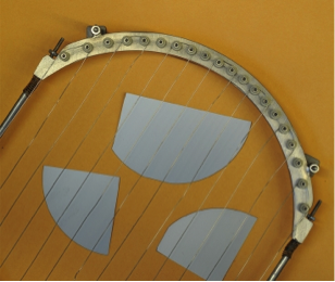
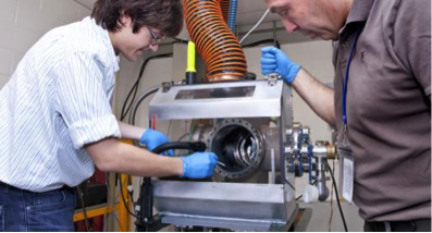
Custom Feedthrough Assemblies
Rigaku offers custom-engineered solutions from simple feedthroughs to feedback controlled subsystems for managing motion. This includes function-enhanced products and clean/vacuum magnetic rotary seals for robots.
|
|
From AR Coatings to Notch Filters, and from TCOs to DBRs, Evatec offers customized coating platforms and complete process solutions based on enhanced evaporation and sputter.
Phone: (603) 669-9656
www.evatecnet.com
E-Mail:infoNA@evatecnet.com
|
64 CFM List $8,250
3 to 64 CFM, 6 to 108 m3/hour. All voltages, 1 and 3 phase. Fomblim/Krytox available. 2 year parts & labor warranty, satisfaction guaranteed.Prices and Complete Specs at:
|
SVC TechCon Exhibitor
Visit Us at Booth 312
Fil-Tech's New 2013 Catalog
Fil-Tech's Quality Crystals®
Gold, Longer Life Gold, and Alloy 6MHz and 5MHz styles. Fil-Tech supplies rate monitors, sensorheads, feedthroughs, ebeam and ion source parts. Fil-Tech's FT704 replaces DC704. Call for catalog and Technical Bulletins.
Fil-Tech, Inc.
617-227-1133 or 800-743-1743
www.filtech.com
|

THREE STEPS TO SUCCESS
Power Mag Technologies now offers 3 different power levels of DC Magnetrons to enhance your sputtering process with the Maxim line of power supplies.
Contact: 877.513.3295
|

Thin-Films Research is prepared to meet your custom thin-film coating requirements. Using state-of-the-art equipment and over 40 years of experience, Thin-Films Research offers technology for the electro-optics, semiconductors, sensors & medical electronic industries. Learn More
Thin-Films Research, Inc.
270 Littleton Road
Westford, MA 01886
Phone: 978-692-9530
Fax: 978-692-9531
E-Mail: sales@thinfilmsresearch.com |
SVC TechCon Exhibitor
Visit Us at Booth 702
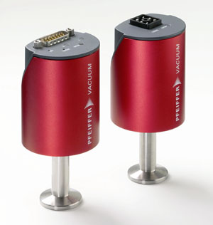
CMR ActiveLine Vacuum Gauges
Pfeiffer Vacuum CMR capacitance manometers offer compact and rugged vacuum measurement from 10-5 to 1100 mbar. A ceramic sensor prevents memory effect and resists corrosive gases. Learn More.
Pfeiffer Vacuum, Inc.
Phone: 800-248-8254
Web site: www.pfeiffer-vacuum.com
contact@pfeiffer-vacuum.com
|
|
Smart solutions for surface technology from Bürkert - perfect for optimal process yields, high quality and peace of mind.
Bürkert. We make ideas flow.
Bürkert Werke GmbH
Maik Lösel
Segment Manager Gas Handling
Christian-Bürkert-Str. 13-17
74653 Ingelfingen, Germany
Phone: +49 35952 36 362
Email: maik.loesel@burkert.com
|
The Hiden HPR-30 is a residual gas analyser configured for analysis of gases and vapours in vacuum processes and for vacuum diagnostics.
Learn more.
|
|
Temescal Systems & Components
Industry leaders choose Temescal for our unparalleled expertise in electron beam coating system and component solutions. Embrace the cloud.
Learn more.
http://www.temescal.net
(800) 522-1215
email: temescalinfo@ferrotec.com
|
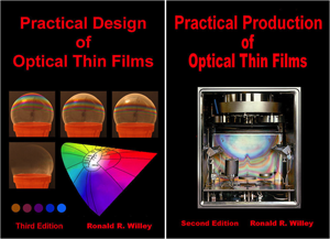
One-week Course in the Practical Design and Production of Optical Thin Films
June 3-7, 2013
Also
October 14-18, 2013
Charleviox, MI USA
Comprehensive and Comprehensible!
|
SVC TechCon Exhibitor
Visit Us at Booth 621

USB-Powered Reflectometer for Thin-Film Measurement
Quickly measure thickness and index of single- and multi-layer films using aRTie, which simultaneously measures reflectance and transmittance.
Learn more.
Filmetrics, Inc.
Phone: 858-573-9300
www.filmetrics.com
info@filmetrics.com
|
SVC TechCon Exhibitor
Visit Us at Booth 827
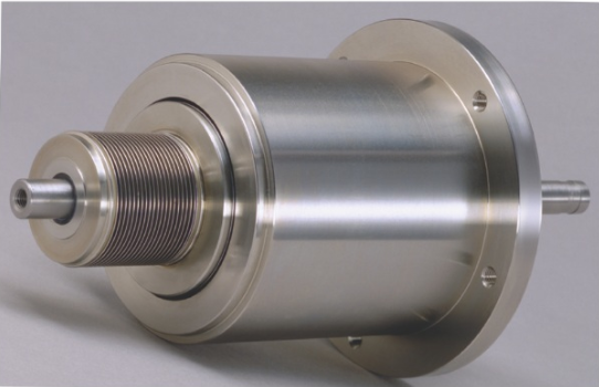
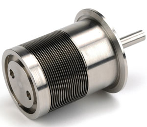
Ferrofluidic Seals
Ferrotec's Ferrofluidic® vacuum feedthroughs set the standard for precision sealing in rotary motion applications. Available in standard sizes or customized for your requirements. Learn more.
http://seals.ferrotec.com
(800) 258-1788
email: info@ferrotec.com
|
Versatile and Reliable Vacuum Deposition Systems (e-beam and thermal evaporation, ion beam and magnetron sputtetring) for Universities and industry, components for PVD and sputtering systems. ROBVAC Fryazino, Moscow Region, Russia Tel: +7 495 966 2814 www.robvac.com |
SVC TechCon Exhibitor
Visit Us at Booth 212

Polycold™ and Telemark™ Refrigerant Charges YTI offers prompt delivery of Polycold and Telemark refrigerant at dramatically lower costs than buying direct. Replacement refrigerant is available for PCT, P. PFC, PGC and 2 series units. Learn More. YTI Vacuum Coating
Equipment and Service
Phone: 860.429.1908
refrigerant@ytionline.com
www.ytionline.com
|

Providence, Rhode Island
50 miles south of Boston, MA
Technical Program - April 22-25
|

NEW!
SVC Vacuum Coating Resource Guide
in partnership with Multiview
The on-line Vacuum Coating Resource Guide replaces the Product and Services Locators on the SVC Web Site. This innovative, dynamic resource provides users current information for product and service providers in our technology.
Is your company listed in the
Vacuum Coating Resource Guide?
Contact Multiview to enhance your listing in the Guide or to purchase high-profile advertising space. in the Guide or to purchase high-profile advertising space. |
|
|

|
|
Researchers Solve Riddle: What Holds Two Unlikely Materials Together
| From North Carolina State University, March 11, 2013:
"For years, researchers have developed thin films of bismuth telluride (Bi2Te3) - which converts heat into electricity or electricity to cooling - on top of gallium arsenide (GaAs) to create cooling devices for electronics. But while they knew it could be done, it was not clear how - because the atomic structures of those unlikely pair of materials do not appear to be compatible. Now researchers from North Carolina State University and RTI International have solved the mystery, opening the door to new research in the field.
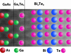
They report the atomic scale structure and chemistry of epitaxial Bi2Te3 thin films grown via metallorganic chemical vapor deposition on (001) GaAs substrates. Using aberration corrected high-angle annular dark-field scanning transmission electron microscopy (HAADF STEM), they report an atomically abrupt interface spanned by a second phase. Further, they demonstrate that interpretation of HAADF STEM image intensities does not provide an unambiguous interface structure. Combining atomic resolution imaging and spectroscopy, they determine the identity of the interfacial species is found to be consistent with that of a bilayer of Ga-Te that terminates GaAs dangling bonds."
|
|
A Cooler Way to Protect Silicon Surfaces
|
From MIT News, February 13, 2013, by David L. Chandler: "Silicon, the material of high-tech devices from computer chips to solar cells, requires a surface coating before use in these applications. The coating "passivates" the material, tying up loose atomic bonds to prevent oxidation that would ruin its electrical properties. But this passivation process consumes a lot of heat and energy, making it costly and limiting the kinds of materials that can be added to the devices. Now a team of MIT researchers has found a way to passivate silicon at room temperature, which could be a significant boon to solar-cell production and other silicon-based technologies.
 Typically, silicon surfaces are passivated with a coating of silicon nitride, which requires heating a device to 400 degrees Celsius. By contrast, the process the team uses decomposes organic vapors over wires heated to 300 C, but the silicon itself never goes above 20 C - room temperature. The new process also has an added benefit, providing an anti-reflective coating that improves a solar cell's overall efficiency. Both the conventional process and the new process take place in a vacuum chamber." Typically, silicon surfaces are passivated with a coating of silicon nitride, which requires heating a device to 400 degrees Celsius. By contrast, the process the team uses decomposes organic vapors over wires heated to 300 C, but the silicon itself never goes above 20 C - room temperature. The new process also has an added benefit, providing an anti-reflective coating that improves a solar cell's overall efficiency. Both the conventional process and the new process take place in a vacuum chamber."
The research was recently published online in the journal Advanced Materials.
Source: Read the full article...
|
|
Near-Perfect Optical Absorber Developed
|
From Photonics Spectra, February 2013: : "A tunable device coated with a film 100 times thinner than the wavelength of incident light 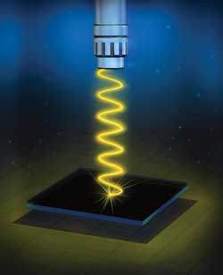 absorbs 99.75 percent of a specific mid-infrared band on demand, potentially expanding thermal detection and energy harvesting applications. Designed by scientists at the School of Engineering and Applied Sciences (SEAS) and the University of California, San Diego, the near-perfect absorber is composed of a 180-nm-thick layer of vanadium dioxide (VO2) on a sheet of sapphire, a standard substrate for growing vanadium dioxide. The SEAS device uses a highly unusual approach to achieve better results. The team exploited a kind of naturally disordered metamaterial, along with thin-film interference effects, to achieve one of the highest absorption rates we've ever seen." absorbs 99.75 percent of a specific mid-infrared band on demand, potentially expanding thermal detection and energy harvesting applications. Designed by scientists at the School of Engineering and Applied Sciences (SEAS) and the University of California, San Diego, the near-perfect absorber is composed of a 180-nm-thick layer of vanadium dioxide (VO2) on a sheet of sapphire, a standard substrate for growing vanadium dioxide. The SEAS device uses a highly unusual approach to achieve better results. The team exploited a kind of naturally disordered metamaterial, along with thin-film interference effects, to achieve one of the highest absorption rates we've ever seen."
Source: Read the full article...
Image: from Photonics Spectra: An artist's rendition of the experimental setup used to measure the reflectivity of the Harvard SEAS and University of California, San Diego, perfect absorber researchers created using unusual materials and interference effects.
|
2013 SVC TechCon Promotional Partners
|
The following publications and organizations are playing an important role promoting the 2013 SVC TechCon within and outside the vacuum coating community. 
Association of Vacuum Equipment Manufacturers (AVEM): The Association of Vacuum Equipment Manufacturers (AVEM) is the only U.S. Association dedicated completely to companies that manufacture vacuum equipment and supplies that serve and advance vacuum science and technology. AVEM was founded in 1969 and is the only non-profit source for market data across the vacuum industry. Visit us at www.avem.org.
See all the 2013 SVC TechCon Promotional Partners Here. If you are Interested in promoting the SVC 2013 TechCon to your readers or members, contact publications@svc.org for details on becoming a Promotional Partner. |
|
Better SEM Imaging and Measurements in the Nano Era
| From NIST, March 14, 2013: "Since the inception of the scanning electron microscope (SEM), users have encountered the persistent problem of contamination. Cleanliness is required for imaging and to make good quality measurements, and the Physical Measurement Lab has led the exploration and the development of methods to allow SEM users gather high-quality, repeatable, and quantitative measurement results. Users can now measure the exact features of the sample, not the sample features plus a layer of contamination.
C harged particle beam-induced contamination in SEMs manifests itself as a gradual buildup of carbonaceous material on the surface of the sample where the ions or electrons are focused, resulting in characteristic dark patterns. Such contamination changes the sample, as well as the number, trajectory, and energy of the electrons leaving the sample, making repeatable quantitative measurements difficult or impossible. Researchers have developed a modified plasma-cleaning device that works in a wide vacuum range and also has higher power, up to 99 watts. While low power is sufficient for oxygen-based plasma cleaning, oxygen-sensitive samples (for example evaporated gold on carbon resolution samples, which can be damaged by oxygen gas) need hydrogen or helium plasma cleaning, where higher power is very helpful. Their work has led to a NIST Contamination Specification, steps that SEM users worldwide can take to determine whether their instruments need to be cleaned and how to implement an effective cleaning process." harged particle beam-induced contamination in SEMs manifests itself as a gradual buildup of carbonaceous material on the surface of the sample where the ions or electrons are focused, resulting in characteristic dark patterns. Such contamination changes the sample, as well as the number, trajectory, and energy of the electrons leaving the sample, making repeatable quantitative measurements difficult or impossible. Researchers have developed a modified plasma-cleaning device that works in a wide vacuum range and also has higher power, up to 99 watts. While low power is sufficient for oxygen-based plasma cleaning, oxygen-sensitive samples (for example evaporated gold on carbon resolution samples, which can be damaged by oxygen gas) need hydrogen or helium plasma cleaning, where higher power is very helpful. Their work has led to a NIST Contamination Specification, steps that SEM users worldwide can take to determine whether their instruments need to be cleaned and how to implement an effective cleaning process."
|
|
Gaining Insight into HIPIMS Technology with Patent Study
|
From Fraunhofer Institute for Surface Engineering and Thin Films IST, Germany: "Basic research into HIPIMS technology received increasing interest around the turn of the millenium, and Fraunhofer Institute for Surface Engineering and Thin Films IST has carried out a patent study to give a comprehensive insight into the patent situation in this field.The study offers all relevant patent data from the field of HIPIMS technology, combining wide-ranging solutions in a condensed and easily readable survey and providing a comprehensive overview of the patent landscape, focusing on the relevant aspects of R&D work. The study is updated permanently, providing the reader with information about new patents continuously.
|
|
Thermal Spray Coating: Characterization and Evaluation
|
From Advanced Materials & Processes, February 2013, Vol. 171,
No. 2, by Douglas G. Puerta (IMR Test Labs): "Despite increased efforts in training and education, areas such as metallographic preparation of thermal spray coatings remains without standardization. Furthermore, the aerospace industry has struggled to adopt a common set of definitions to evaluate coatings. Therefore, features such as oxides and porosity may be rated differently depending on the specification being used. Other common ASTM tests such as bond strength and hardness, can also show inconsistent results due to variables associated with bonding agents or preparation methods. Because of this general lack of training and standardization, the person applying and/or evaluating a given coating often rates it differently than the end user, which can lead to incorrect rejection of good coatings, resulting in additional costs and lead times for rework."
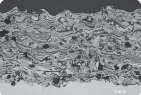 This article reviews the four major steps in thermal spray coating sample preparation for metallographic examination (sectioning, mounting, grinding and polishing) as well as hardness and adhesion testing, and describes how following best practices will assure accurate representation of the true coating structure. This article reviews the four major steps in thermal spray coating sample preparation for metallographic examination (sectioning, mounting, grinding and polishing) as well as hardness and adhesion testing, and describes how following best practices will assure accurate representation of the true coating structure.
Source: Read the full article...
|
|
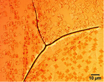
Improved "Peacock" Technology
|
From University of Michigan, February 5, 2013: "Iridescence, or sheen that shifts color depending on your viewing angle, is pretty in peacock feathers. But it's been a nuisance for engineers trying to mimic the birds' unique color mechanism to make high-resolution, reflective, color display screens. Now, researchers at the University of Michigan have found a way to lock in so-called structural color, which is made with texture rather than chemicals.
 The researchers etched nanoscale grooves in a plate of glass with the technique commonly used to make integrated circuits, or computer chips. Then they coated the grooved glass plate with a thin layer of silver. When light-which is a combination of electric and magnetic field components-hits the grooved surface, its electric component creates what's called a polarization charge at the metal slit surface, boosting the local electric field near the slit. That electric field pulls a particular wavelength of light in. A paper on the work is published online in the current edition of the Nature journal Scientific Reports."
Source: Read the full article... The researchers etched nanoscale grooves in a plate of glass with the technique commonly used to make integrated circuits, or computer chips. Then they coated the grooved glass plate with a thin layer of silver. When light-which is a combination of electric and magnetic field components-hits the grooved surface, its electric component creates what's called a polarization charge at the metal slit surface, boosting the local electric field near the slit. That electric field pulls a particular wavelength of light in. A paper on the work is published online in the current edition of the Nature journal Scientific Reports."
Source: Read the full article...
|
Routes Towards Defect-Free Graphene
| From University of Oxford, UK, February 1, 2013:
"A team led by Oxford University scientists has overcome a key problem of growing graphene when using CVD, that the tiny flakes of graphene form with random orientations, leaving defects or 'seams' between flakes that grow together. The discovery, reported in a paper published in ACS Nano, reveals how these graphene flakes, known as 'domains', can be lined up by manipulating the alignment of carbon atoms on a relatively cheap copper foil - the atomic structure of the copper surface acts as a 'guide' that controls the orientation of the carbon atoms growing on top of them."
|
|
Light-Emitting Triangles of Tungstenite
|
From Penn State News, February 5, 2013: "For the first time, scientists have created single layers of a naturally occurring rare mineral called tungstenite, or WS2. The resulting sheet of stacked sulfur and tungsten atoms forms a honeycomb pattern of triangles that have been shown to have unusual light-emitting, or photoluminescent, properties. The triangular  structures have potential applications in optical technology; for example, for use in light detectors and lasers. Creating monolayers is of special interest to scientists because the chemical properties of minerals and other substances are known to change depending on their atomic thickness, opening the door to potentially useful applications of multi-layered materials of various thicknesses. structures have potential applications in optical technology; for example, for use in light detectors and lasers. Creating monolayers is of special interest to scientists because the chemical properties of minerals and other substances are known to change depending on their atomic thickness, opening the door to potentially useful applications of multi-layered materials of various thicknesses.
The team used CVD process with the rare mineral called tungstenite. The scientists began by depositing tiny crystals of tungsten oxide and then passed the crystals through sulfur vapor at 850 degrees Celsius. This process led to individual layers -- or sheets -- composed of one atom in thickness. The resulting structure -- called tungsten disulfide -- is a honeycomb pattern of triangles consisting of tungsten atoms bonded with sulfur atoms."
The results of the research will be published in a print edition of the journal NANO Letters.
|
|
Plasma Meets Nano at PPPL
|
From Princeton Plasma Physics Lab (PPPL), February 13, 2013, by John Greenwald:
"Scientists at the U.S. Department of Energy's (DOE) Princeton Plasma Physics Laboratory (PPPL) have launched a new effort to apply expertise in plasma to study and optimize the use of the hot, electrically charged gas as a tool for producing nanoparticles. This research aims to advance the understanding of plasma-based synthesis processes, and could lead to new methods for creating high-quality nanomaterials at relatively low cost."
 "PPPL researchers have launched a nanotechnology laboratory that they envision as a step toward research capabilities that could serve as a resource for institutions and industries around the world. The facility will explore so-called low-temperature plasmas that are frequently used to synthesize nanomaterials. The production of nanomaterials involves complex transitions between different states of matter when plasma serves as a synthesizing medium. PPPL researchers will seek to better understand these interactions to conduct controllable synthesis of nanomaterials with precisely prescribed properties." "PPPL researchers have launched a nanotechnology laboratory that they envision as a step toward research capabilities that could serve as a resource for institutions and industries around the world. The facility will explore so-called low-temperature plasmas that are frequently used to synthesize nanomaterials. The production of nanomaterials involves complex transitions between different states of matter when plasma serves as a synthesizing medium. PPPL researchers will seek to better understand these interactions to conduct controllable synthesis of nanomaterials with precisely prescribed properties."
Source: Read the full article...
Princeton Plasma Physics Lab:
Image: Elle Starkman, PPPL Office of Communications
|
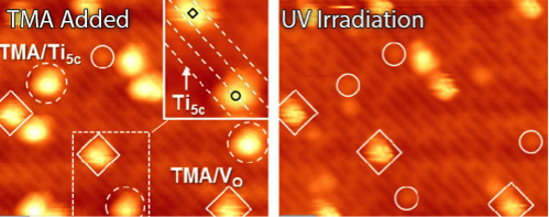
Titanium Dioxide Surface Defects Halt Photodecomposition
| From Pacific Northwest National Laboratory (PNNL), February 2013: "Using chemical imaging techniques, scientists at Pacific Northwest National Laboratory proved for the first time that titanium dioxide's surface defects shelter chemicals from decays caused by ultra-violet light. The defects are tiny gaps created when oxygen atoms are missing from the surface of this popular catalyst. Conventional wisdom says the vacancies are more active than the surface. The team showed the opposite is true for photooxidation. The carbon-based carboxylic group, trimethyl acetate (TMA), remains intact if bound in the vacancies while it readily decomposes at regular, or non-vacancy, sites on the surface. Titanium dioxide is used in dye-sensitized solar cells, self-cleaning windows, and other devices."
Source: Read the full article...
|
|
Nanopaper Transistors for Flexible and Transparent Electronics
| From Nanowerk Spotlight, February 21, 2013:
"Recently, cellulose papers have been explored to replace plastic substrates as a lightweight substrate for low-cost, versatile, and roll-to-roll printed electronics. Researchers have already demonstrated various types of devices on papers such as batteries, solar cells, or RFID tags. A research group at the University of Maryland, has now fabricated transistors on specially designed nanopaper. Reporting their findings in a recent online edition of ACS Nano ("Highly Transparent and Flexible Nanopaper Transistors"), the researchers show that flexible organic field-effect transistors (OFETs) with high transparency and excellent mechanical properties can be fabricated on tailored nanopapers."
Source: Read the full article...
Nanowerk: Click Here.
Image: University of Maryland, Bing Research Group
|
|
Rechargeable Battery Can Stretch, Twist, and Bend
|
From Northwestern University, February 26, 2013, by Megan Fellman: "Researchers at Northwestern University and the University of Illinois are the first to demonstrate a stretchable lithium-ion battery -- a flexible device capable of powering their innovative stretchable electronics. No longer needing to be connected by a cord to an electrical outlet, the stretchable electronic devices now could be used anywhere, including inside the human body. 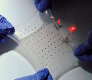 The power and voltage of the stretchable battery are similar to a conventional lithium-ion battery of the same size, but the flexible battery can stretch up to 300 percent of its original size and still function. The battery continues to work -- powering a commercial light-emitting diode (LED) -- even when stretched, folded, twisted and mounted on a human elbow. The battery can work for eight to nine hours before it needs recharging, which can be done wirelessly." The power and voltage of the stretchable battery are similar to a conventional lithium-ion battery of the same size, but the flexible battery can stretch up to 300 percent of its original size and still function. The battery continues to work -- powering a commercial light-emitting diode (LED) -- even when stretched, folded, twisted and mounted on a human elbow. The battery can work for eight to nine hours before it needs recharging, which can be done wirelessly."
Source: Read the full article...
|
|
Do You Have an Interesting Article to Share?
|
Interested in sharing the latest news in vacuum coating technology? Forward us a link to an article you want to share with the rest of the SVC readership to publications@svc.org. Purchase advertising space in this newsletter by contacting SVC at  svcinfo@svc.org. svcinfo@svc.org.
Society of Vacuum Coaters
71 Pinon Hill Place NE
Albuquerque, New Mexico 87122
505-856-7188
|
|
|
|
|