ULVAC's SPW-030 roll coating system is capable of processing 300 mm wide substrate compositions including thin-gauge metal rolls and polymeric materials for R&D and Pilot-scale production. Learn More.
ULVAC Technologies, Inc. Visit Us Online Tel: 1-978-686-7550
E-mail: sales@us.ulvac.com |
|
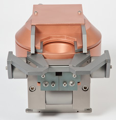
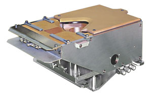
Multi-Hearth Electron Beam Source
The YTI ULTRA SOURCE retains all the advantages of the Sloan e-beam source: large hearth capacity, high deposition rates, long filament life, and reliability, but has been re-engineered for improved productivity and uptime. Learn More.
YTI Thin Film Products and Services
Phone: 860.429.1908
www.ytionline.com
|

INFICON thin film deposition controllers, monitors and accessories, including customizable sensors and feedthroughs, offer features, function and value targeted to your application. View our catalog and contact us today! |
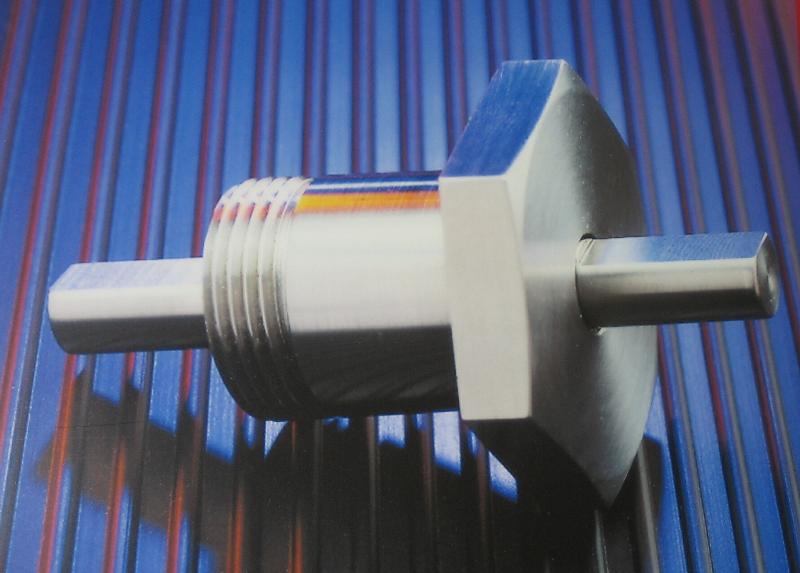
Reliable, Low Cost Rotary Motion Feedthroughs
Rigaku solid-shaft Superseal rotary motion feedthroughs are the ultimate value, rotary sealing solution. They are the lowest cost feedthroughs while being recognized for their quality and performance. Learn More.
|
Got a Handle on Destructive Arcing? Comdel Can Help.
Comdel's VF Series Multiple Channel Synthesizers provide phase adjustable output to avoid destructive arcing and cross-talk in multiple cathode plasma processing chambers, and allows adjustment for cable length dependencies. Learn more.
|
|
From AR Coatings to Notch Filters, and from TCOs to DBRs, Evatec offers customized coating platforms and complete process solutions based on enhanced evaporation and sputter.
Phone: (603) 669-9656
www.evatecnet.com
E-Mail:infoNA@evatecnet.com
|
7CFM OEM Price $1047
3 to 64 CFM, 6 to 108 m3/hour. All voltages, 1 and 3 phase. Fomblim/Krytox available. 2 year parts & labor warranty, satisfaction guaranteed.
|
Fil-Tech's Quality Crystals® Gold, Longer Life Gold, and Alloy 6MHz and 5MHz styles. Fil-Tech supplies rate monitors, sensorheads, feedthroughs, ebeam and ion source parts. Fil-Tech's FT704 replaces DC704. Call for catalog and Technical Bulletins.
Fil-Tech, Inc. 617-227-1133 or 800-743-1743 www.filtech.com |

THREE STEPS TO SUCCESS
Power Mag Technologies now offers 3 different power levels of DC Magnetrons to enhance your sputtering process with the Maxim line of power supplies.
Contact: 877.513.3295
|
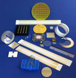
Thin-Films Research is prepared to meet your custom thin-film coating requirements. Using state-of-the-art equipment and over 40 years of experience, Thin-Films Research offers technology for the electro-optics, semiconductors, sensors & medical electronic industries. Learn More
Thin-Films Research, Inc.
270 Littleton Road
Westford, MA 01886
Phone: 978-692-9530
Fax: 978-692-9531
E-Mail: sales@thinfilmsresearch.com |

$4,995 Dry Turbopump Station
The Pfeiffer Vacuum HiCube™ Eco vacuum station includes turbo and dry diaphragm pumps. It delivers a pumping speed of 67 l/s and an ultimate pressure of <10-8 mbar. Learn More.
Pfeiffer Vacuum, Inc.
24 Trafalgar Square
Nashua, NH 03063-1988
Phone: 603-578-6500
contact@pfeiffer-vacuum.com
|
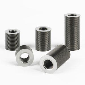
Easily Purchase AM 350 Metal Bellows Online
Use 350 AM edge welded bellows from Bellowstech for demanding UHV applications. Available in a large variety of diameters at the most competitive prices. Visit the Bellowstech online store today.
BellowsTech, LLC
Phone: 386-615-7530
Fax: 386-615-7973
Email: bellows@bellowstech.com
|

Smart solutions for surface technology from Bürkert - perfect for optimal process yields, high quality and peace of mind.
Bürkert. We make ideas flow.
Bürkert Werke GmbH
Maik Lösel
Segment Manager Gas Handling
Christian-Bürkert-Str. 13-17
74653 Ingelfingen, Germany
Phone: +49 35952 36 362
Email: maik.loesel@burkert.com
|
The Hiden HPR-30 is a residual gas analyser configured for analysis of gases and vapours in vacuum processes and for vacuum diagnostics.
Learn more.
|
|
Ferrofluidic Seals
Ferrotec's Ferrofluidic® vacuum feedthroughs set the standard for precision sealing in rotary motion applications. Available in standard sizes or customized for your requirements. Learn more.
http://seals.ferrotec.com
(800) 258-1788
email: info@ferrotec.com
|
|
Temescal Systems & Components
Industry leaders choose Temescal for our unparalleled expertise in electron beam coating system and component solutions. Embrace the cloud.
Learn more.
http://www.temescal.net
(800) 522-1215
email: temescalinfo@ferrotec.com
|
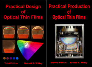
One-week Course in the Practical Design and Production of Optical Thin Films
June 3-7, 2013
Charleviox, MI USA
Comprehensive and Comprehensible!
|

Next Live Webinar
"Evaporation for
Thin Film Deposition"
Thursday, February 28, 2013
9:00 am - Noon, Mountain Time
with S. Ismat Shah
University of Delaware
Register Now
Space is Limited
___________________________
Explore the entire SVC Webinar library, both Live and On-Demand Formats
Learn More!
|
|
|

|
|
Edges Ease Surface Oxidation of Metals
|
From Chemical & Engineering News, December 17, 2012, by Jyllian Kemsley: "Oxidation of metal surfaces preferentially occurs when metal atoms detach form defect edges and react with adsorbed oxygen atoms. By using transmission electron microscopy to study oxidation of copper surfaces under low-pressure oxygen, a research group at the State University of New York, Binghamton, determined that oxidation occurs 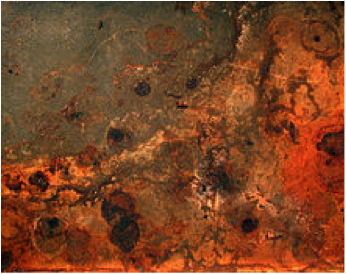 as oxygen adsorbs onto the surface and reacts with copper atoms that detach from step edges and diffuse across the surface. The team found that oxidizing a flat surface leads to more stress and mechanical breakdown between the metal and oxide layers, while step-facilitated oxidation reduces stress and smooths the surface as metal atoms are drawn from the edges." as oxygen adsorbs onto the surface and reacts with copper atoms that detach from step edges and diffuse across the surface. The team found that oxidizing a flat surface leads to more stress and mechanical breakdown between the metal and oxide layers, while step-facilitated oxidation reduces stress and smooths the surface as metal atoms are drawn from the edges." This report is in the journal, Physical Review Letters, (DOI: 10.1103/ physrevlett.109.235502) Source: Read the full article... Chemical & Engineering News: http://cen.acs.org/articles/90/i51/Edges-Ease-Surface-Oxidation-Metals.html Image: Wikimedia Commons, Roger McLassus
|
|
Novel Approaches to Thermal Spray
|
From Advanced Materials & Processes, November/December 2012, by Rajan Bamola: " New thermal spray methods to apply functional oxide coatings have been developed. Many require crossover technology like chemical or physical vapor deposition (CVD or PVD). The most well-known cross-over technology in thermal spray is Sulzer Metco's (Switzerland) very low pressure plasma spray (VLPPS), also referred to as plasma spray PVD. PVD thermal barrier coatings have better strain tolerance compared with air plasma spray (APS) coatings. Besides gas turbine applications, researchers are investigating VLPPS coatings for solid fuel cells, biomedical components, and electronics. Thin-film 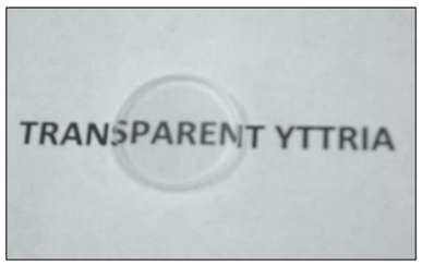 thermal spray CVD is of particular interest in semiconductor field where dense, well-adhering thin films of special oxides such as yttria are of interest for plasma erosion resistance and corrosion resistance against halogen attack." thermal spray CVD is of particular interest in semiconductor field where dense, well-adhering thin films of special oxides such as yttria are of interest for plasma erosion resistance and corrosion resistance against halogen attack."
Source: Read the full article...
|
|
Deformable Mirrors Enable a Leap Forward in X-Ray Telescope Performance
|
From SPIE Newsroom, January 7, 2013, by Vincenzo Cotroneo: "Space-based x-ray telescopes allow astronomers to study a wide range of energetic phenomena from neutron stars to diffuse million-degree gas permeating galaxy clusters. Unfortunately, x-rays are notoriously difficult to focus. To produce images, x-ray telescopes must use grazing incidence mirrors, which reflect incoming photons at very shallow angles. High-resolution x-ray mirrors usually use the Wolter Type I geometry-a double reflection off first a parabolic and then a hyperbolic surface. As a consequence of the shallow angles (typically 1° or less), the collecting area is a small fraction of the mirror surface. To increase the telescope's effective area, multiple mirror pairs are nested. Thin mirrors can be nested in higher number and more densely than thicker 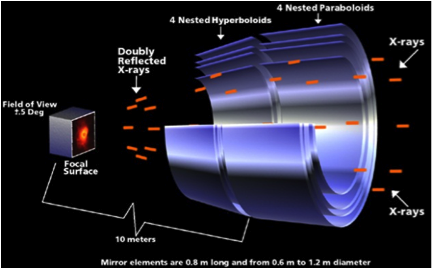 mirrors, resulting in a large total collecting area, but they are more subject to manufacturing and mounting errors that degrade the angular resolution." mirrors, resulting in a large total collecting area, but they are more subject to manufacturing and mounting errors that degrade the angular resolution."
Source: Read the full article...
Image: NASA/Chandra/Smithsonian Astrophysical Observatory
|
2013 SVC TechCon Promotional Partners
|
The following publications and organizations are playing an important role promoting the 2013 SVC TechCon within and outside the vacuum coating community.

Photonics Media - the Pulse of the Industry - invites you to explore the information leader and all that we have to offer. As the publisher of Photonics Spectra, BioPhotonics and EuroPhotonics magazines, Photonics Buyers' Guide, Photonics.com, and more, we bring you the news, research and applications articles you need to succeed. Visit www.Photonics.com for your FREE subscriptions and much more.
See all the 2013 SVC TechCon Promotional Partners Here. If you are Interested in promoting the SVC 2013 TechCon to your readers or members, contact publications@svc.org for details on becoming a Promotional Partner. |
|
Peel and Stick Solar Panels
|
From Stanford University, December 19, 2012, by Glen Martin:
" Stanford researchers have succeeded in developing the world's first peel-and-stick thin-film solar cells. Unlike standard thin-film solar cells, peel-and-stick thin-film solar cells do not require any direct fabrication on the final carrier substrate. This is a far more dramatic development than it may initially seem. All the challenges associated with putting solar cells on unconventional materials are avoided with the new process, vastly expanding the potential applications of solar technology. 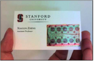
Nonconventional or 'universal' substrates are difficult to use for photovoltaics because they typically have irregular surfaces and they don't do well with the thermal and chemical processing necessary to produce today's solar cells. Stanford researchers got around these problems by developing this peel-and-stick process, which gives thin-film solar cells flexibility and attachment potential we've never seen before, and also reduces their general cost and weight. They didn't lose any of the original cell efficiency."
Source: Read the full article...
Stanford University School of Engineering: http://engineering.stanford.edu/news/peel-stick-solar-panels-stanford-engineering
Image: Stanford University School of Engineering
|
|
Ultra-Thin Coatings Change Color with Few Atoms Difference in Thickness
|
From Harvard University, October 2012, by Caroline Perry: "Harvard physicists have discovered that very "lossy" thin films, if atomically thin, can be tailored to reflect a particular range of dramatic and vivid colors. The structure made of only two elements, gold and  germanium (or many other possible pairings), can be whatever color one chooses. The germanium film is applied through standard manufacturing techniques-lithography and physical vapor deposition, so with only a minimal amount of material (a thickness between 5 and 20 nanometers), elaborate colored designs can easily be patterned onto any surface, large or small." germanium (or many other possible pairings), can be whatever color one chooses. The germanium film is applied through standard manufacturing techniques-lithography and physical vapor deposition, so with only a minimal amount of material (a thickness between 5 and 20 nanometers), elaborate colored designs can easily be patterned onto any surface, large or small."
The work is published in the journal Nature Materials (online).Source: Read the full article...
Image: Mikhail Kats, Romain Blanchard, and Patrice Genevet
|
|
Electrodynamic Dust Shield on the International Space Station
| |
From NASA, Kennedy Space Center, December 2012, by C.I. Calle:
"Electrodynamic Dust Shields (EDS) have been in development at NASA as a dust mitigation method for lunar and Martian missions. Dust mitigation technologies are high on list of requirements for these planetary bodies, since they covered with layers of dust that can interfere with the operation of equipment, rovers, habitats spacesuits, and resource processing plants. They report on the development of a flight experiment to fully expose four EDS panels to the space environment.
The EDS uses traveling electric fields to transport electrostatically charged particles along surfaces. To generate the traveling electric fields, the EDS consists of a multilayer dielectric coating with an embedded thin electrode grid running a multiphase low frequency AC signal. Electrically charged particles are carried along by the traveling field due to action of coulomb and dielectrophoretic forces.
The EDS multilayer coating is applied to metallic and electrically insulating surfaces. EDS with vapor-deposited metallic electrodes are used for metallic surfaces, such as astronaut helmets. For optical systems, transparent, vapor-deposited ITO electrodes are used."
Source: Read the full article...
|
|
Production and Processing of Graphene and 2D Crystals
|
From Materials Today, December 2012 by Francesco Bonaccorso:
New applications for graphene require development of reliable and inexpensive commercial manufacturing processes. This article reviews current graphene processes for preparation, manufacturing, and handling. Manufacturing processes include CVD, MBE, and ALE (atomic layer epitaxy). Other 2d crystals and hybrids have similar properties to graphene. In addition to utilizing graphene's manufacturing processes, 2d crystal thin films are produced by PVD and magnetron sputtering.
Source: Read the full article...
|
Carbon Nanotubes Used for Electronic Interconnects
|
From Georgia Institute of Technology, October 2012, by John Toon:
"Using a new method for precisely controlling the deposition of carbon, researchers at Georgia Institute of Technology have demonstrated a technique for connecting multi-walled carbon nanotubes to the metallic pads of integrated circuits without the high interface resistance produced by traditional fabrication techniques. Based on electron beam-induced deposition (EBID), the work is believed to be the first to connect multiple shells of a multi-walled carbon nanotube to metal terminals on a semiconducting substrate, which is relevant to integrated circuit fabrication. Using this three-dimensional fabrication technique, researchers developed graphitic nanojoints on both ends of the multi-walled carbon nanotubes, which yielded a 10-fold decrease in resistivity in its connection to metal junctions.
 The research was supported by the Semiconductor Research Corporation, and in its early stages, by the National Science Foundation. The work was reported online in the journal IEEE Transactions on Nanotechnology." The research was supported by the Semiconductor Research Corporation, and in its early stages, by the National Science Foundation. The work was reported online in the journal IEEE Transactions on Nanotechnology."
Source:
Georgia Institute of Technology: http://gtresearchnews.gatech.edu/low-resistance-connections-cnt/
Image: Gary Meek
|
|
2013 Global R&D Funding Forecast
|
From R&D Magazine, December 2012, by Martin Grueber: " R&D Magazine and Batelle present the latest forecast of global research and development funding and trends, including the annual survey of researchers for their challenges, issues and opportunities. This article examines: 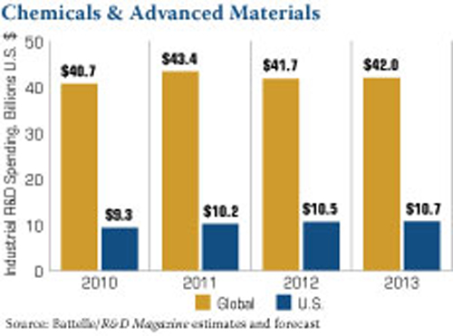 - Leading U.S. R&D Firms
- U.S. Industry Perspectives
- U.S. and Global Industry Forecast
- Materials Innovation Enabling Research in Other Sectors
- Creating A Global Materials Network
|
|
How Transparent is Graphene?
|
From MIT News, December 4, 2012, by David L. Chandler: "
The "transparency" of a graphene coating to wetting is not as absolute as some researchers had thought. New research at MIT shows that for materials with intermediate wettability, graphene does preserve the properties of the underlying material. But for more extreme cases, superhydrophobic or superhydrophilic surfaces, an added layer of graphene does significantly change the way coated materials behave. Most electrically conductive materials are hydrophilic. On the other hand, for many electronic and military applications, it is important to fabricate hydrophobic, electrically conductive surfaces. And while graphene's transparency to wettability is not perfect, it may still be good enough for such applications.
 This research shows that by depositing a large graphene sheet, grown by CVD process, on another material's surface, it would be possible to induce electrical conductivity on the surface, while partially preserving the desired surface wetting behavior. They have demonstrated that the wettability of a transparent, graphene-coated surface can be manipulated without undermining its thermal/electrical conductivity." This research shows that by depositing a large graphene sheet, grown by CVD process, on another material's surface, it would be possible to induce electrical conductivity on the surface, while partially preserving the desired surface wetting behavior. They have demonstrated that the wettability of a transparent, graphene-coated surface can be manipulated without undermining its thermal/electrical conductivity."
The work is published in the journal Physical Review Letters.
Source: Read the full article...
MIT News:
Image: Chih-Jen Shih
|
Stretchable Electronics and Electrics for Electric Vehicles
| From IDTechEx, December 28, 2012, by Dr. Peter Harrop: "This article shares some of the research in the newly updated IDTechEx report, "Stretchable Electronics Comes to Market". Flexible electronics is typically printed reel to reel and it is typically rollable around a 2.5 centimeter diameter, newer versions in the laboratory being rollable around a human hair.
However, this flexible electronics is barely stretchable and its flexibility is usually only in one dimension at a time. In the automotive industry and particularly with electric vehicles for land, water and air, something more is preferable - three dimensional stretchability. It is needed both for producing rigid products by stretching them to form during plastic molding and it is useful in a form that is stretchable in use."
Source: Read the full article...
|
|
Stretchable Energy Storage Devices
| From University of Delaware, December 11, 2012, by Karen B. Roberts:
"According to the University of Delaware's Bingqing Wei, stretchable electronics are the future of mobile electronics, leading giants such as IBM, Sony and Nokia to incorporate the technology into their products. Advances in soft and stretchable substrates and elastomeric materials have given rise to an entirely new field. Rechargeable and stretchable energy storage devices, also known as supercapacitors, are urgently needed to complement advances currently being made in flexible electronics.
 The research group at the University is making significant progress in developing scalable, stretchable power sources for this type of application using carbon nanotube macrofilms, polyurethane membranes and organic electrolytes. To reveal a stretchable supercapacitator's true performance, the Wei group examined the system's electrochemical behavior using buckled single-wall nanotube (SWNT) electrodes and an elastomeric separator. The supercapacitor developed in his lab achieved excellent stability in testing." The research group at the University is making significant progress in developing scalable, stretchable power sources for this type of application using carbon nanotube macrofilms, polyurethane membranes and organic electrolytes. To reveal a stretchable supercapacitator's true performance, the Wei group examined the system's electrochemical behavior using buckled single-wall nanotube (SWNT) electrodes and an elastomeric separator. The supercapacitor developed in his lab achieved excellent stability in testing."
The work was recently published in the journal Nano Letters.
Source: Read the full article...
|
|
DOE Selects Ames Laboratory to Lead Research Addressing Rare-Earth Material Shortages
| From US Department of Energy, January 9, 2013: "The U.S. Department of Energy announced today that a team led by Ames Laboratory in Ames, Iowa, has been selected for an award of up to $120 million over five years to establish an Energy Innovation Hub that will develop solutions to the domestic shortages of rare earth metals and other materials critical for U.S. energy security. The new research center, which will be named the Critical Materials Institute (CMI), will bring together leading researchers from academia, four Department of Energy national laboratories, as well as the private sector.
Rare earth metals and other critical materials are essential to manufacturing wind turbines, electric vehicles, advanced batteries and a host of other products. These materials are part of the "Critical Materials Strategy" including five rare earth metals (dysprosium, terbium, europium, neodymium and yttrium) that may affect clean energy technology deployment in the coming years."
Source: Read the full article...
|
|
Do You Have an Interesting Article to Share?
|
Interested in sharing the latest news in vacuum coating technology? Forward us a link to an article you want to share with the rest of the SVC readership to publications@svc.org. Purchase advertising space in this newsletter by contacting SVC at  svcinfo@svc.org. svcinfo@svc.org.
Society of Vacuum Coaters
71 Pinon Hill Place NE
Albuquerque, New Mexico 87122
505-856-7188
|
|
|
|
|