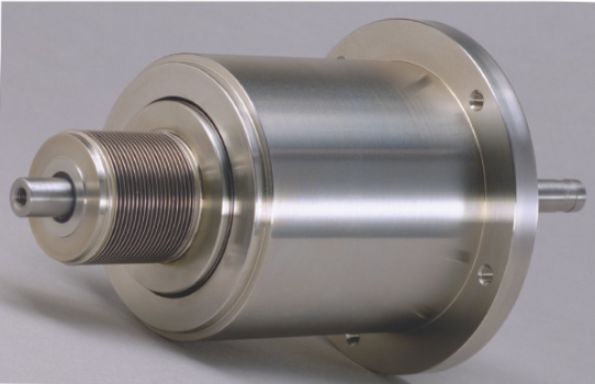
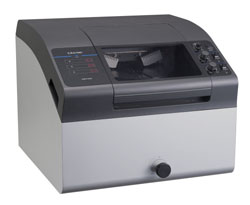
EQP Mass and Energy Analyser for Plasma Diagnostics
- Plasma ion analyser for +ve and -ve ion analysis
- Neutrals and neutral radical detection
- For correlation of plasma parameters with film quality Learn More
|

VAT's REAL L-MOTION VALVE
For SEMI and LED
Check out VAT's redesigned website for the latest news about VAT's 450mm Transfer Valves and other VAT happenings. Visit us at AVS in Florida!
Contact Us:
Phone: 781-935-1446
or 800-935-1446
|
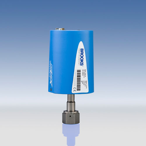
Capacitance Manometers that Last
...Up to 3x Longer
The rugged design of the Brooks XacTorr handles byproduct build-up, lasting up to three times longer even in aggressive processes. Learn more.
Brooks Instrument
Phone: 215.362.3700
Email:
BrooksAM@BrooksInstrument.com
|
High Speed Compact Ellipsometer
The ULVAC UNECS Spectroscopic Ellipsometer measures thin film thickness and optical constants faster (20 ms/point) and more efficiently than conventional mechanically controlled rotating optical devices. Learn More.
ULVAC Technologies, Inc.
Visit Us Online
Tel: 1-978-686-7550
E-mail: sales@us.ulvac.com
|

Polycold™ and Telemark™ Refrigerant Charges YTI offers prompt delivery of Polycold and Telemark refrigerant charges at dramatically lower costs than buying direct. Replacement charges are available for PCT, P. PFC, PGC and 2 series units. Learn More. YTI Thin Film Products and Services
Phone: 860.429.1908
charges@ytionline.com
www.ytionline.com
|

INFICON thin film deposition controllers, monitors and accessories, including customizable sensors and feedthroughs, offer features, function and value targeted to your application. View our catalog and contact us today! |
Custom Feedthrough Assemblies
Rigaku offers custom-engineered solutions from simple feedthroughs to feedback controlled subsystems for managing motion. This includes function-enhanced products and clean/vacuum magnetic rotary seals for robots.
|
Got a Handle on Destructive Arcing? Comdel Can Help.
Comdel's VF Series Multiple Channel Synthesizers provide phase adjustable output to avoid destructive arcing and cross-talk in multiple cathode plasma processing chambers, and allows adjustment for cable length dependencies.Learn more.
Comdel
11 Kondelin Road
Gloucester, MA 01930
Tel: 978-282-0620 or 800-468-3144
info@comdel.com |
|
From AR Coatings to Notch Filters, and from TCOs to DBRs, Evatec offers customized coating platforms and complete process solutions based on enhanced evaporation and sputter.
Phone: (603) 669-9656
www.evatecnet.com
E-Mail:infoNA@evatecnet.com
|
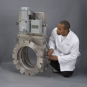
Large Throttle Valves
Throttle Valves with ports as large as 630 mm, ISO-630 or ANSI 24 inch. Also any flange style as small as NW-25. Aluminum, steel or stainless steel.
Vacuum Research Corporation Phone: 800/426-9340
Web: www.vacuumresearch.com
E-Mail: vrc@vacuumresearch.com
|
Fil-Tech's Quality Crystals® Gold, Longer Life Gold, and Alloy 6MHz and 5MHz styles. Fil-Tech supplies rate monitors, sensorheads, feedthroughs, ebeam and ion source parts. Fil-Tech's FT704 replaces DC704. Call for catalog and Technical Bulletins.
Fil-Tech, Inc. 617-227-1133 or 800-743-1743 www.filtech.com |

Solid Sealing Technology designs and manufactures hermetic assemblies using metalizing, brazing and glass-ceramic sealing including standard and custom Feedthroughs/Connectors for extreme environments and UHV.
Contact:
Ph: 518-874-3600
Fax: 518-874-3610
info@solidsealing.com
|

THREE STEPS TO SUCCESS
Power Mag Technologies now offers 3 different power levels of DC Magnetrons to enhance your sputtering process with the Maxim line of power supplies.
Contact: 877.513.3295
|
Thin-Films Research is prepared to meet your custom thin-film coating requirements. Using state-of-the-art equipment and over 40 years of experience, Thin-Films Research offers technology for the electro-optics, semiconductors, sensors & medical electronic industries. Learn More
Thin-Films Research, Inc.
270 Littleton Road
Westford, MA 01886
Phone: 978-692-9530
Fax: 978-692-9531
E-Mail: sales@thinfilmsresearch.com |

$4,995 Dry Turbopump Station
The Pfeiffer Vacuum HiCube™ Eco vacuum station includes turbo and dry diaphragm pumps. It delivers a pumping speed of 67 l/s and an ultimate pressure of <10-8 mbar. Learn More.
Pfeiffer Vacuum, Inc.
24 Trafalgar Square
Nashua, NH 03063-1988
Phone: 603-578-6500
contact@pfeiffer-vacuum.com
|

Next Live Webinar
"Troubleshooting for Thin Film Deposition Processes"
Tuesday, December 11, 2012
9:00 am - Noon, Mountain Time
with Gary S. Ash
Castle Brook Corporation
Register Now
Space is Limited
___________________________
Explore the entire SVC Webinar library, both Live and On-Demand Formats
Learn More!
|
|
|
|
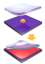
Stacked Nanoparticle Layers Shine New Light on Optical Thin Films
|
From Nanowerk Spotlight, November 5, 2012, by Michael Berger, Copyright © Nanowerk: "Work by researchers at National Taiwan University is reported in the online edition of Advanced Functional Materials ("Nanoparticle Stacks with Graded Refractive Indices Enhance the Omnidirectional Light Harvesting of Solar Cells and the Light Extraction of Light-Emitting Diodes"). They have not only demonstrated lower reflectivity but also provided a strategy for optimizing the types and sizes of nanoparticles for use in both solar cells and LEDs." The most common material used in today's commercial solar cells is silicon and has a high refractive index which causes more than 30% of incident light to be reflected back from the surface of the silicon wafer.
Source: Read the full article...
Nanowerk: http://www.nanowerk.com/spotlight/spotid=27180.php#ixzz2CeuzPKxU
|
|
All-Carbon Solar Cell Could be Used in Photovoltaic Devices
|
From Stanford Report, October 31, 2012, by Mark Shwartz: "Stanford University scientists have built the first solar cell made entirely of carbon, a promising alternative to the expensive materials used in photovoltaic devices today. The results are published in the journa  l ACS Nano. Unlike rigid silicon solar panels that adorn many rooftops, Stanford's thin film prototype is made of carbon materials that can be coated from solution. Study senior author Zhenan Bao, a professor of chemical engineering at Stanford said, 'Perhaps in the future we can look at alternative markets where flexible carbon solar cells are coated on the surface of buildings, on windows or on cars to generate electricity.' The Bao group's experimental solar cell consists of a photoactive layer, which absorbs sunlight, sandwiched between two electrodes. In a typical thin film solar cell, the electrodes are made of conductive metals and indium tin oxide (ITO). 'Materials like indium are scarce and becoming more expensive as the demand for solar cells, touchscreen panels and other electronic devices grows,' Bao said. 'Carbon, on the other hand, is low cost and Earth-abundant.'"
Source: Read the full article...
|
|
Roll-to-Roll Plasma Etch System Development Project Completed
|
From Flex Tech Alliance, October 17, 2012: "FlexTech Alliance, focused on developing the flexible and printed electronics industry supply chains, announced the completion of a development project with Etched in Time, Inc. (EITI), for a plasma etch system that is compatible with a wide array of roll-to-roll equipment. The result of the project is a tool that can be used in the manufacture of a broad range of products including LED lighting or solar panels fabricated on plastic substrates. The purpose of this FlexTech Alliance funded project was to create a plasma etching tool for dielectric films that offers a number of manufacturing advantages for flexible electronics. For example, plasma etching is cleaner than a wet etching manufacturing process due to the lack of chemicals to dispose after use. Additionally, incorporating the system into a roll-to-roll process allows large area and flexible products to be fabricated at low cost."
Source: Read the full article...
|
2013 SVC TechCon Promotional Partners
|
The following publications and organizations are playing an important role promoting the 2013 SVC TechCon within and outside the vacuum coating community.

Laser Focus World is a global media resource for engineers, researchers, scientists, and technical managers, providing comprehensive global coverage of optoelectronic and photonic technologies, applications, and markets. LFW reports on and analyzes the latest developments and significant trends in both technology and business in the worldwide optoelectronics and photonics industry. Visit http://www.laserfocusworld.com/index.html
See all the 2013 SVC TechCon Promotional Partners Here. If you are Interested in promoting the SVC 2013 TechCon to your readers or members, contact publications@svc.org for details on becoming a Promotional Partner.
|
|
IBM Fabricates Carbon Nanotubes as Successor to Silicon in Computer Chips
|
From IBM, October 28, 2012: "IBM scientists have demonstrated a new approach to carbon nanotechnology that opens up the path for commercial fabrication of dramatically smaller, faster and more powerful computer chips. For the first time, more than ten thousand working transistors made of nano-sized tubes of carbon have been precisely placed and tested in a single chip using standard semiconductor processes. These carbon devices are poised to replace and outperform silicon technology allowing further miniaturization of computing components and leading the way for future microelectronics.
 IBM researchers developed a novel method based on ion-exchange chemistry that allows precise and controlled placement of aligned carbon nanotubes on a substrate at a high density - two orders of magnitude greater than previous experiments, enabling the controlled placement of individual nanotubes with a density of about a billion per square centimeter." Source: Read the full article... IBM Newsroom: http://www-03.ibm.com/press/us/en/pressrelease/39250.wss Image: IBM
|
|
Scientists Use Molecular Layers to Study Nanoscale Heat Transfer
|
From Eurekalert, October 26, 2012: "A research team at the University of Illinois at Urbana-Champaign (UIUC) has developed a novel system for examining and measuring nanoscale thermal conductance at the interface between two materials. With further refinement, the scientists believe their advance may one day provide data for applications such as harvesting electricity from waste heat, better cooling of microelectronic devices and "heat-seeking" targeting of disease cells by hyperthermal (above normal body temperature) therapeutics.
At the nanoscale, thermal properties are the result of vibrations between neighboring atoms. Bonds between atoms carry these vibrations similar to an oscillating spring. The UIUC team developed a technique for studying the effects of these bonds on heat transport across an interface between two different materials."
The team's findings were presented at the recent AVS 59th International Symposium and Exhibition. Source: Read the full article...
|
|
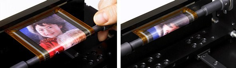
Global Flexible Display Market Worth $3,298 Million by 2017
|
From MarketsandMarkets: The total market for flexible display is expected to reach $3,298 million by 2017 "according to a new market research report, 'Flexible Display Market: Global Analysis & Forecast (2012 - 2017) By Application (Smartphone, Tablet, e-reader, Laptop, TV, Smartcard, Wearable Display, e-label), Technology (OLED, LCD, e-paper), Component (Substrate, Layers, & Others) & Geography' published by MarketsandMarkets.
The shipment of flexible display in various applications is expected to reach 223.40 million units by 2017. America is the leading region in the overall flexible display market; followed by Europe and APAC . In rest of the world, Middle East, and Africa are the largest contributors."
Source: Read the full article...
|
|
GaAs on Graphene Hybrid for Optoelectronics
|
From Compound Semiconductor, September 10, 2012.: " CrayoNano is introducing GaAs nanowires on graphene, a patented hybrid material with competitive properties. Semiconductors grown on graphene are expected to become the basis for new types of device systems, and could fundamentally change the semiconductor industry.
The new patented hybrid material offers excellent optoelectronic properties, says Helge Weman, CTO and co-founder of CrayoNano AS. "We have managed to combine low cost, transparency and flexibility in our new electrode," he adds. The patented method of growing semiconductor nanowires on atomically thin graphene employs MBE to  grow the nanowires. Researchers see this is a template for a new production method for semiconductor devices." grow the nanowires. Researchers see this is a template for a new production method for semiconductor devices."
Results are published in Nano Letters.Source: Read the full article...
|
|
NASA's Relationship with Nanotechnology
|
From Rice University's Baker Institute for Public Policy, October 2012: "Rice University's Baker Institute of Public Policy has released a report, "NASA's Relationship with Nanotechnology: Past, Present and Future Challenges", which "reviews the history of nanotechnology R&D at NASA over the past 15 years. Nanotechnology serves as an ideal case study of emerging technology development in NASA's long struggles to translate research projects into viable technologies."
"NASA R&D experienced resurgence in funding totaling $9.8 billion in FY2012, a 6 % increase from FY2010. In FY2013, NASA restructured its science budget, adding the Space Technology Mission Directorate (STMD), which focuses on "developing breakthrough space capabilities and applications," including several nano-based research initiatives. In addition to NASA's increased investment in early-stage "game-changing technologies," National Nanotechnology Initiative reports a 29 percent increase in NASA nanotechnology-specific R&D in 2012 - from $17 million in 2011 to $23 million in 2012 - that was put toward developing next-generation nanomaterials and nanoscale systems."
The National Academies reviewed NASA's "Space Technology Roadmaps" including the nanotechnology roadmap. "Using the National Academies' recommendations, NASA plans to establish both short-term (3-5 year) and long-term (20-30 year) plans for all basic and applied R&D at its research facilities and flight centers."
Read NASA's Draft 2010 Nanotechnology Roadmap: http://www.nasa.gov/pdf/501325main_TA10-Nanotech-DRAFT-Nov2010-A.pdf
Source:
Baker Institute for Public Policy at Rice University: www.bakerinstitute.org/policyreport54
|
|
SPTS Technologies, Fraunhofer IZM Researching Lower-Temp Films for Through-Silicon Vias
|
From ElectroIQ, October 18, 2012, by James Montgomery:
"SPTS Technologies has signed a joint development program with the Fraunhofer Institute for Reliability and Microintegration (Fraunhofer-Institut für Zuverlässigkeit und Mikrointegration, IZM) and its All Silicon System Integration Dresden (ASSID) center, to investigate sub-175°C dielectric films in through-silicon vias (TSV) for 3D IC packaging.
 ASSID, created in 2010 to develop 300mm-based 3D integration technologies, will use 300mm PECVD modules installed on a Versalis platform alongside SPTS etch chambers. Integrating the PECVD modules with etch processes on a single wafer handler will optimize process results and reduce capital expenditure for development and pilot production, the firms claim. ASSID, created in 2010 to develop 300mm-based 3D integration technologies, will use 300mm PECVD modules installed on a Versalis platform alongside SPTS etch chambers. Integrating the PECVD modules with etch processes on a single wafer handler will optimize process results and reduce capital expenditure for development and pilot production, the firms claim.
SPTS' advanced process module (APM) enables low-temperature PECVD for via-last applications and via-reveal passivation; depositing dielectric layers for TSV isolation at lower temperatures (<175°C) provides high sidewall coverage, low stress, and "in-via" electrical performance. For via reveal, the APM offers high deposition rate silicon oxide and nitride films compatible with silicon-on-glass substrates with what the company says are excellent coverage, barrier properties, and electrical isolation."
Source: Read the full article... ElectroIQ: http://www.electroiq.com/articles/ap/2012/10/spts-technologies-fraunhofer-izm-researching-lower-temp-films-for-tsvs.html Image: SPTS
|
|
Beautiful Physics: Tying Knots in Light
|
From Australian National University, October 26, 2012: "Dr. Anton Desyatnikov from the Nonlinear Physics Centre at The Australian National University is part of an international team of scientists who are designing knots in light, with potential applications in advanced modern optics, laser beams and even quantum computing. Using concepts from mathematics and physics the model Dr. Desyatnikov and his colleagues have explored creates optical vortices with dark cores in a bright laser beam, that can then tangle and form links and knots.
'Apart from their curiosity value, what's really interesting and useful about these knots of darkness is that they show you what the power flow is doing,' Dr. Desyatnikov said. 'It is part of the incredible progress science is making in the field of optics, we're beginning to do things with light that would have once seemed impossible. The really interesting thing is that we can't predict exactly where they will form. Just that under these specific circumstances the optical vortices will spontaneously nucleate and tie themselves into little knots.'"
Their work is published in Scientific Reports.
Source: Read the full article... Australian National University:
Image: Australian National University
|
|
Tweaking Growth of Oxide Thin Films Key to Novel Materials
| From Oak Ridge National Laboratory, November 19, 2012:
"By tweaking the formula for growing oxide thin films, researchers at the Department of Energy's Oak Ridge National Laboratory achieved virtual perfection at the interface of two insulator materials. This finding, published in the journal Advanced Materials, could have significant ramifications for creation of novel materials with applications in energy and information technologies, leading to more efficient solar cells, batteries, solid oxide fuel cells, faster transistors and more powerful capacitors. The research team, led by ORNL's Ho Nyung Lee, demonstrated that a single unit cell layer of lanthanum aluminate grown on a strontium titanate substrate is sufficient to stabilize a chemically and atomically sharp interface. A unit cell is the smallest group of atoms that possess the properties of a crystalline material."
Source: Read the full article...
|
|
New Technology for Semiconductor Film Production on Highly Liquid-Repellent Surfaces
| From Phys.org, November 15, 2012: "Japanese researchers have developed a manufacturing technology for highly uniform thin films of organic polymer semiconductors without material losses by applying the semiconductor solution on a highly hydrophobic surface that strongly repels the solution. The technology allows remarkably simple production of high performance thin-film transistors (TFTs) that are indispensable building blocks for information terminal devices such as electronic papers.
 In this study, the researchers developed a new "push coating" technique to produce organic polymer semiconductor films on highly hydrophobic surfaces, where a solution of organic polymer semiconductor is compressed with an original silicone-rubber-based trilayer stamp to wet the hydrophobic surfaces uniformly by way of the capillarity. The technique allows the production of uniform and highly crystalline semiconductor thin films on hydrophobic surfaces. It causes almost no material loss, in striking contrast to any other solution processes. Improved crystallinity of the films was confirmed using the synchrotron radiation facilities at the High Energy Accelerator Research Organization (KEK; Director General: Atsuto Suzuki). It is expected that the developed technology would greatly accelerate the research and development of flexible electronic devices, and also that the technology should be applicable to thin-film processing of a wide range of materials.
Source: Read the full article...
|
|
Do You Have an Interesting Article to Share?
|
Interested in sharing the latest news in vacuum coating technology? Forward us a link to an article you want to share with the rest of the SVC readership to publications@svc.org. Purchase advertising space in this newsletter by contacting SVC at  svcinfo@svc.org. svcinfo@svc.org.
Society of Vacuum Coaters
71 Pinon Hill Place NE
Albuquerque, New Mexico 87122
505-856-7188
|
|
|
|
|