New Report: Advanced Patterning 2008 to 2013
|
Linx Consulting is pleased to release Advanced Patterning 2008 To 2013. The new report is the second update of Linx's Advanced Patterning Report and includes market forecasts from 2008 to 2013 for patterning materials.
Lithography is facing an uncertain future as EUV once touted for HVM by 2012 has now been delayed to 2016, well into the 16nm node. High index lithography, once a promising technology, has fallen out of favor due to issues of costs, technology readiness, and seemingly insurmountable scientific challenges. The immediate implication of these industry shortcomings is that immersion 193nm lithography involving pitch doubling (double patterning) and ancillary resist materials will continue to play a critical role in sustaining Moore's Law for the next eight years, down to the 22nm node.
Double Patterning
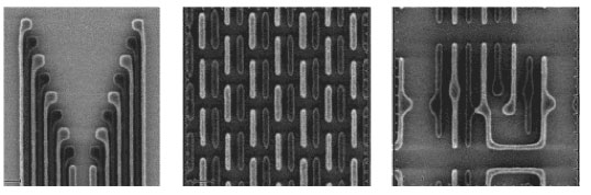
Logic device vendors and research consortia continue to improve and implement immersion lithography in volume manufacturing for 4X nodes. However the path to achieving finer patterns at 3X and 2Xnm nodes remains complex. Interaction between equipment, materials, and processes used in pattern transfer is still a major challenge. Flash vendors have made progress in implementing CVD-based self-aligned double patterning (SADP) based on spacers for 3Xnm. But the path for flash to 2X and 1X nodes remains murky. The vacuum deposited films add a new factor to the lithography marketplace, and brings new competitive players and opportunities to what has traditionally been a spin-on market.
This updated report presents:
� The technology and materials employed in both spin-on and CVD-based patterning.
� Market forecasts from 2008 to 2013 for patterning materials as well as the key market drivers.
� Emerging trends, opportunities, and critical issues for manufacturers and end users of materials and ancillaries for IC patterning. Read More....
For more information on Advanced Patterning 2008 - 2013, call Mark Thirsk at 617.273.8837 or send him an email.
|
|
| Linx Consulting will be at SPIE Advanced Lithography in San Jose
|
Linx Consulting will be at SPIE Advanced Lithography in San Jose from February 23 - 26 to address customer inquiries. If you would like to set up a meeting to review Advanced Patterning, 2008 - 2013 or any of our reports or services, please contact us directly.
Dr. Armah M. Kpissay, Linx Consulting Senior Analyst
akpissay@linx-consulting.com
Cell: 857-272-7037
Mark Thirsk, Managing Partner
mthirsk@linx-consulting.com
Cell:774-245-0959
|
|
Linx Offers Custom Services in Addition to Electronic Materials Reports
|
Linx Consulting offers other reports on the Electronic Materials Industry. If you don't find exactly what you're looking for in a Linx report, we can design a custom report for your company to address your unique decision-making needs.
Call us at 973.698.2331 or send us an email us at info@linx-consulting.com for more information.
|