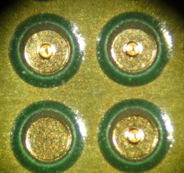
|
Getting Via in Pad Right the First Time!
There are numerous reasons you may want to use via-in-pad designs. These reasons may include all /some of the following:
- They can allow really close placement of bypass capacitors,
- They can help with thermal management-especially on BTCs,
- They can make routing easier with fine pitch or large IO count BGAs,
- They can help with grounding on high-frequency parts and
- As a percentage, the RLC characteristics of the via-in-pad are significantly better than traditional designs.
Using a via-in-pad design presents the challenge of voiding in the laminate during the assembly process. Voids can create expansion and/or contraction with temperature variation during board operation. The expansion/contraction creates stress on the via walls which can lead to interconnection problems.

If you must use via-in-pad make sure the vias are plugged or capped at the board house. Have your board fab house plug the via and then plate copper over it. They can plug using a thermally and electrically conductive epoxy before the final plating steps. This will give you all of the benefits of via in pad without causing problems in assembly. Another way of dealing with this is to cap the underside of the board with solder mask. This will usually stop the solder from completely wicking down the via, but sometimes the cap can pop open and sometimes the void is big enough to still suck too much of the solder off of the pad. It can even suck down the solder ball off of the BGA leaving an open. Component-side solder mask via caps aren't the best way to deal with a via in pad situation, but it can work reasonably well for BTC (bottom terminated component) packages.Capping the bottom side will usually keep the solder from leaching out onto the secondary side of the PCB, but several other problems can occur. Outgassing from the solder paste can cause the cap to come off during reflow, leaving you with an open via. Finally, make sure your PCB fabricator gets the flatness of the board right. Ask them about how they will control and measure the flatness of the resulting pad. Some PCB fabricators plug and plate over or cap a via in a pad but do not deliver a flat surface. If the board shop cannot hold the flatness of the pad this will be a big problem , especially with the smaller pitch (ie 0.5mm and below) BGAs. An indent can lead to insufficient solder under that ball and a bump can tilt the part, leading to poor connections under other balls. Call BESTProto at (847) 797-9250 for further guidance or ask our opinion prior to assembly.
|