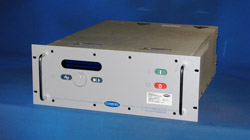
Comdel's CV Series Delivers Stable Power for VHF Applications
Comdel's CV series offers stable power at frequencies from 30 to 80 MHz. Ideal for use in VHF plasma systems, solar/photovoltaics, CW and pulsed laser systems. Learn more.
Comdel
11 Kondelin Road
Gloucester, MA 01930
Tel: 978-282-0620 or 800-468-3144
Fax: 978-282-4980
www.comdel.com
info@comdel.com
|
TechCon Exhibitor
Visit Us at Booth 316 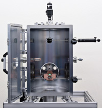 MDC's Bundled Engineered Solutions MDC offers virtually every component required for vacuum coating applications. With MDC's standard chamber line you have the advantage of bundling these high quality pieces together without hours or weeks of special engineering. More... MDC engineered process solutions www.mdcvacuum.com |
TechCon Exhibitor
Visit Us at Booth 606
From AR Coatings to Notch Filters, and from TCOs to DBRs, Evatec offers customized coating platforms and complete process solutions based on enhanced evaporation and sputter.
Phone: (603) 669-9656
www.evatecnet.com
E-Mail:infoNA@evatecnet.com
|
| TechCon Exhibitor Visit Us at Booth 705 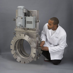
Large Throttle Valves
Throttle Valves with ports as large as 630 mm, ISO-630 or ANSI 24 inch. Also any flange style as small as NW-25. Aluminum, steel or stainless steel.
Phone: 800-426-9340
Web: vacuumresearch.com
|
TechCon Exhibitor Visit Us at Booth 211 
Dynavac produces a wide range of thin film deposition systems that include electron beam, thermal evaporation, sputtering and ion-assist. Our reputation is built upon quality, reliability, and excellent customer relations.
Telephone: 781-740-8600 |
TechCon Exhibitor Visit Us at Booth 607 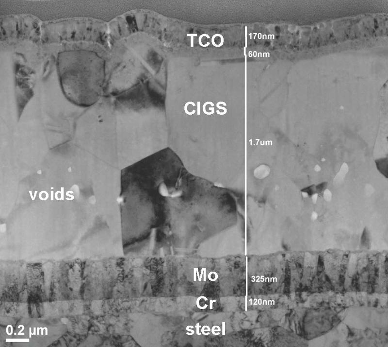
Evans Analytical Group (EAG) is the leading global provider of high quality surface analysis and materials characterization services to the films and coatings industry.
Evans Analytical Group
1.800.366.3867
|
TechCon Exhibitor Visit Us at Booth 837 
Solid Sealing Technology designs and manufactures hermetic assemblies using metalizing, brazing and glass-ceramic sealing including standard and custom Feedthroughs/Connectors for extreme environments and UHV.
Contact:
Ph: 518-874-3600
Fax: 518-874-3610
info@solidsealing.com
|
Thin-Films Research is prepared to meet your custom thin-film coating requirements. Using state-of-the-art equipment and over 40 years of experience, Thin-Films Research offers technology for the electro-optics, semiconductors, sensors & medical electronic industries. Learn More
Thin-Films Research, Inc.
270 Littleton Road
Westford, MA 01886
Phone: 978-692-9530
Fax: 978-692-9531
E-Mail: sales@thinfilmsresearch.com |
TechCon Exhibitor Visit Us at Booth 310

Roots Pumping Stations
Pfeiffer Vacuum CombiLine™ Roots Pumping Stations optimize industrial coating processes in pressure ranges from atmosphere to high vacuum. They include all pumps, gauges, analytical equipment and control systems.
Learn More.
Pfeiffer Vacuum, Inc.
24 Trafalgar Square
Nashua, NH 03063-1988
Phone: 603-578-6500
combiline@pfeiffer-vacuum.com
|
TechCon Exhibitor Visit Us at Booth 616 
VAT manufactures high quality vacuum valves for a variety of applications. Products include: gate, angle, fast-closing, transfer, pendulum, throttle, pressure control, all-metal and customized valves. Learn more.
Contact Us:
Phone: 781-935-1446
or 800-935-1446
E-Mail: US@vatvalve.com
|
TechCon Exhibitor Visit Us at Booth 942 
Capacitance Manometers that Last
...Up to 3x Longer
The rugged design of the Brooks XacTorr handles byproduct build-up, lasting up to three times longer even in aggressive processes. Learn more.
Brooks Instrument
Phone: 215.362.3700
Email:
BrooksAM@BrooksInstrument.com
|

Polycold™ & Telemark™
Installation and Service For over 20 years YTI has installed and serviced Polycold™ and Telemark™ cryogenic refrigeration systems. Emergency field service is performed 24/7 by factory-certified technicians. Learn More. YTI Thin Film Products & Services Phone: (860) 429-1908 E-Mail: info@ytionline.com
|
TechCon Exhibitor Visit Us at Booth 617 
INFICON thin film deposition controllers, monitors and accessories, including customizable sensors and feedthroughs, offer features, function and value targeted to your application. View our catalog and contact us today! |
TechCon Exhibitor
Visit Us at Booth 106 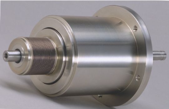
Custom Feedthrough Assemblies
Rigaku offers custom-engineered solutions from simple feedthroughs to feedback controlled subsystems for managing motion. This includes function-enhanced products and clean/vacuum magnetic rotary seals for robots. Learn More.
Rigaku Vacuum Products
E-mail: vacuum-info@rigaku.com
Phone: 603-890-6001
|

COMING THIS MONTH!
April 28 - May 3, 2012
Santa Clara, California
Early Bird Registration Ends April 5
Register Today
Exhibit
Education
Networking
Connect to TechCon MOBILE and explore the TechCon from your Mobile Device
|
|
|

|
|
U.S. DOE Releases 2011 Critical Materials Strategy
|
From Energy.gov, December 22, 2011: The DOE has released the latest edition of its Critical Materials Strategy examining the role of rare earth metals and other materials in the clean energy economy. "The 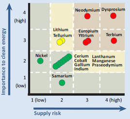 2011 report includes updated criticality assessment, market analyses and technology analyses to identify critical materials challenges. It was prepared by the U.S. Department of Energy (DOE) based on data collect and research performed during 2011. The report highlights are: 2011 report includes updated criticality assessment, market analyses and technology analyses to identify critical materials challenges. It was prepared by the U.S. Department of Energy (DOE) based on data collect and research performed during 2011. The report highlights are:
- Several clean energy technologies - including electric vehicles, PV thin films and fluorescent lighting - use materials at risk of supply disruptions in the short term. Risks will generally decrease in the medium and long term.
- Supply challenges for five rare earth metals (dysprosium, terbium, europium, neodymium and yttrium) may affect clean energy technology deployment in the years ahead.
- In the past year, DOE and other stakeholders have scaled up work to address these challenges. This includes new funding for priority research, development of DOE's first critical materials research plan, international workshops bringing together leading experts and substantial new coordination among federal agencies working on these topics.
- Building workforce capabilities through education and training will help address vulnerabilities and realize opportunities related to critical materials.
- Much more work is required in the years ahead. "
Read the full report for analyses details and DOE's future strategies to address these challenges. Full report is at http://energy.gov/sites/prod/files/DOE_CMS2011_FINAL_Full.pdf. Source: Read the full article... Energy.gov: http://energy.gov/articles/department-energy-releases-its-2011-critical-materials-strategy Image: U.S. Department of Energy
|
|
Sealing Materials for Use in Vacuum at High Temperatures
|
From NASA Tech Briefs, March 1, 2012: "Sealing materials that can be applied and left in place in vacuum over a wide range of temperatures (especially temperatures of a few thousand degrees Celsius) have been conceived and investigated for potential utility in repairing thermal-protection tiles on the space shuttles in orbit before returning to Earth.  These materials are also adaptable to numerous terrestrial applications that involve vacuum processing and/or repair of structures that must withstand high temperatures. These materials can be formulated to have mechanical handling characteristics ranging from almost freely flowing liquid- like consistency through paste-like consistency to stiff putty-like consistency, and to retain these characteristics in vacuum until heated to high curing temperatures." These materials are also adaptable to numerous terrestrial applications that involve vacuum processing and/or repair of structures that must withstand high temperatures. These materials can be formulated to have mechanical handling characteristics ranging from almost freely flowing liquid- like consistency through paste-like consistency to stiff putty-like consistency, and to retain these characteristics in vacuum until heated to high curing temperatures."
Source: Read the full article...
NASA Tech Briefs: http://www.techbriefs.com/component/content/article/13044
Image: NREL
|
|
High-Performance Mirrors Excel for Intracavity Applications
|
From Laser Focus World, February 1, 2012, by Neil Anderson and Ramin Lalezari: "High-performance mirrored optics are an enabling technology in a variety of high-sensitivity measurement techniques such as cavity-based absorption spectroscopy, optical atomic-clock spectroscopy, ring-laser gyroscopes (RLGs), and gravitational-wave detection. In each technique, high-reflectivity, low-loss mirrors that can operate under a variety of environmental conditions without any sacrifice in spectral performance are critical. Here, we describe how mirrors manufactured by ion beam sputtering (IBS) and using dielectric materials are designed to achieve extremely high reflectivity (R) greater than 99.99% and low loss over a broad spectral range. Particular emphasis is given to how the losses associated with light absorption, scattering, and transmission are minimized and quantified by direct measurement. An example of the importance of these mirrors in cavity ring-down spectroscopy (CRDS) will also be discussed."
Source: Read the full article...
|
|
New Form of Hafnium Oxide Developed
|
From University of Cambridge, United Kingdom, February 7, 2012:
"A novel material developed by researchers at the University of Cambridge is opening up new possibilities for next generation electronic and optoelectronic devices, and paving the way for further component miniaturisation.
The material, a new form of hafnium oxide, was developed by Dr Andrew Flewitt's research group in the Department of Engineering. The material provides exceptionally high dielectric constant compared with currently existing forms of hafnium oxide, which is already a key material in the electronics industry.
In order to enable much greater control of the material properties, Dr Flewitt and his team began using a novel deposition technology to promote plasma sputtering. The technology, known as HiTUS (High Target Utilisation Sputtering), was developed by a UK-based company, Plasma Quest Ltd. One of the first materials that the Cambridge team looked at using HiTUS was hafnium oxide."
Source: Read the full article...
|
|
New Technique Lets Scientists Peer Within Nanoparticles, See Atomic Structure in 3-D
|
From UCLA Newsroom, March 21, 2012, by Kim DeRose: "UCLA researchers are now able to peer deep within the world's tiniest structures to create three-dimensional images of individual atoms and their positions. Their research, published March 22 in the journal Nature, presents a new method for directly measuring the atomic structure of nanomaterials.
"This is the first experiment where we can directly see local structures in 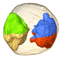 three dimensions at atomic-scale resolution - that's never been done before," said Jianwei (John) Miao, a professor of physics and astronomy and a researcher with the California NanoSystems Institute (CNSI) at UCLA.
Miao and his colleagues used a scanning transmission electron microscope to sweep a narrow beam of high-energy electrons over a tiny gold particle only 10 nanometers in diameter (almost 1,000 times smaller than a red blood cell). The nanoparticle contained tens of thousands of individual gold atoms, each about a million times smaller than the width of a human hair. These atoms interact with the electrons passing through the sample, casting shadows that hold information about the nanoparticle's interior structure onto a detector below the microscope."
Source: Read the full article...
|
|
Researchers Uncover Fundamental Limits on Optical Transparency in Conducting Oxides
|
From University of California Santa Barbara: "Researchers in the Computational Materials Group at the University of California, Santa Barbara (UCSB) have uncovered the fundamental limits on optical transparency in the class of materials known as transparent conducting oxides. Their discovery will support development of energy efficiency improvements for devices that depend on optoelectronic technology, such as light-emitting diodes and solar cells.
Transparent conducting oxides are used as transparent contacts in a 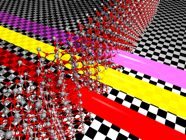 wide range of optoelectronic devices, such as photovoltaic cells, light-emitting diodes (LEDs), and LCD touch screens. These materials are unique in that they can conduct electricity while being transparent to visible light. For optoelectronic devices to be able to emit or absorb light, it is important that the electrical contacts at the top of the device are optically transparent. Opaque metals and most transparent materials lack the balance between these two characteristics to be functional for use in such technology." wide range of optoelectronic devices, such as photovoltaic cells, light-emitting diodes (LEDs), and LCD touch screens. These materials are unique in that they can conduct electricity while being transparent to visible light. For optoelectronic devices to be able to emit or absorb light, it is important that the electrical contacts at the top of the device are optically transparent. Opaque metals and most transparent materials lack the balance between these two characteristics to be functional for use in such technology."
Source: Read the full article: University of California Santa Barbara: http://iee.ucsb.edu/news/pr-conducting-oxides
Image: University of California Santa Barbara
|
|
Germanium Lift-Off Masks for Thin Metal Film Patterning
|
From NASA Tech Briefs, March 1, 2012:
"A technique has been developed for patterning thin metallic films that are, in turn, used to fabricate microelectronics circuitry and thin-film sensors. The technique uses germanium thin films as lift-off masks. This requires development of a technique to strip or undercut the germanium chemically without affecting the deposited metal. Unlike in the case of conventional polymeric lift-off masks, the substrate can be exposed to very high temperatures during processing (sputter deposition). The reason why polymeric liftoff masks cannot be exposed to very high temperatures (>100 °C) is because (a) they can become cross linked, making lift-off very difficult if not impossible, and (b) they can outgas nitrogen and oxygen, which then can react with the metal being deposited. Consequently, this innovation is expected to find use in the fabrication of transition edge sensors and microwave kinetic inductance detectors, which use thin superconducting films deposited at high temperature as their sensing elements."
Source: Read the full article...
NASA Tech Briefs: http://www.techbriefs.com/component/content/article/13042
|
|
Semiconductor Fab Equipment Spending to Hit a Record in 2013
|
From Solid State Technology, March 6, 2012: "Semiconductor fab equipment spending will remain flat (0% increase) in 2012, shows SEMI's World Fab Forecast report. But look for a record spend from semiconductor makers in 2013, jumping from $38.85 billion spent in 2012 to $45 billion in 2013.
Eight companies, including Samsung and Intel, will keep their fab equipment spending level above $2 billion in 2012. Key spenders increased their 2012 capex budgets, pushing SEMI's year forecast from negative to flat. Samsung plans to spend at least $41.4 billion overall, with a hefty amount going to capex; Hynix increased spending in 2012 by 23% ($3.75 billion planned); UMC increased spending from to $2.0 billion; Intel increased spending to a historic high of about $12.5 billion.
If macroeconomic factors improve and other companies adjust their capex plans as well, then equipment spending for 2012 could cross into positive territory."
Source: Read the full article...
|
|
Nanostructure Coatings for U.S. Navy Applications
|
From International Thermal Spray and Surface Engineering (iTSSe), February 2012, by George E. Kim et al.: "): "In 1997, two Program Officers began a five-year program at the United States Office of Naval Research (ONR), entitled "Thermal Spray Processing of Nanostructured Coatings." This program was based on the favorable characteristics found in certain bulk nanostructured materials. The objective was to investigate the thesis that nanostructured thermal spray materials, namely alumina-titania, tungsten carbide-cobalt, and chrome carbide-nickel chrome, could impart similar improvements in mechanical/physical properties of thermal spray coatings compared to their conventional counterparts. ONR's intention was to transfer features found in nanostructured bulk materials into coating form and then apply them to extend the service life of components in applications typically beyond limitations of conventional thermal spray materials. 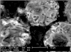
The ONR program produced many successful results. Among them, the work carried out at the University of Connecticut on nanostructured alumina-titania coating, stands out. After 7 years in service, main propulsion shafts in Mine Countermeasure ships showed zero wear of the coating and no signs of spallation. Coatings have also been applied on several Navy components include titanium submarine doors bolted to steel frames and immersed in saltwater, and ball vales that regulate water flow in submarines."
Source: Read the full article...
Advanced Materials and Processing Magazine / iTSSE Newsletter: http://amp.digitaledition.asminternational.org/issue/54544/36
Image: iTSSe
|
|
Chemical Firms Sustain Investments
|
From Chemical and Engineering News (C&EN), February 27, 2012, by Marc Reisch: "Chemical companies plan to increase spending on research and equipment this year but at a slower pace than they did last year. Concerned over the sovereign debt crisis in Europe, a weak economic recovery in the U.S. and a slowdown in the pace of growth in Asia, many chemical executives are tempering their future-oriented spending plans, according to C&EN's annual survey.
 Seventeen U.S.-based firms say they will boost spending on new plants and equipment by 14.1% this year to a combined $13.0 billion. The increase marks a more modest uptick in capital expenditures compared with last year's hefty rise of 31.2% to $11.4 billion. Nonetheless, this year will mark the third annual spending increase after 2009, when investment sank during the great Recession. Eight U.S.-based firms report they will lift their research spending by 3.0% in2012 to a combined $4.4 billion. Seventeen U.S.-based firms say they will boost spending on new plants and equipment by 14.1% this year to a combined $13.0 billion. The increase marks a more modest uptick in capital expenditures compared with last year's hefty rise of 31.2% to $11.4 billion. Nonetheless, this year will mark the third annual spending increase after 2009, when investment sank during the great Recession. Eight U.S.-based firms report they will lift their research spending by 3.0% in2012 to a combined $4.4 billion.
According to C&EN's survey, the overall forecast for future-oriented spending continues to be bright." See further details and data from firms such as Dow Chemical, DuPont, Praxair, 3M and BASF.
Source: Read the full article...
|
|
Nanotube-Based THz Polarizer Leads to New Security, Sensing, Communication Devices
|
From Rice University, January 30, 2012, by Mike Williams: "Researchers at Rice University are using carbon nanotubes as the critical component of a robust terahertz polarizer that could accelerate 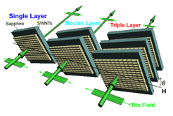 the development of new security and communication devices, sensors and non-invasive medical imaging systems as well as fundamental studies of low-dimensional condensed matter systems.
The polarizer developed by the Rice lab of Junichiro Kono, a professor of electrical and computer engineering and of physics and astronomy, is the most effective ever reported; it selectively allows 100 percent of a terahertz wave to pass or blocks 99.9 percent of it, depending on its polarization. The research was published in the online version of the American Chemical Society journal, Nano Letters. The broadband polarizer handles waves from 0.5 to 2.2 terahertz, far surpassing the range of commercial polarizers that consist of fragile grids wrapped in gold or tungsten wires."
Source: Read the full article... Rice University: http://news.rice.edu/2012/01/30/terahertz-polarizer-nears-perfection-2/ Image: Rice University / Lei Ren
|
|
One Leader, Lots of Consolidation as CIGS Photovoltaic Market Emerges
|
From Renewable Energy World.com, January 25, 2012, by James Montgomery: "2011 was "a breakout year" for CIGS solar PV as suppliers continued to trim production costs, increase module conversion efficiencies, and widen adoption in commercial rooftops. But while CIGS (and thin-film brethren CdTe, thanks to First Solar's market leadership) continue to press on, the solar PV industry is still very much dominated by silicon, which has more standardized manufacturing on the one end and far more installed capacity on the installation side -- and all-important bankability thanks to both.
 CIGS, meanwhile, is still evolving, with a variety of substrates (glass, steel, polyimide) and manufacturing processes e.g. deposition (sputtering, evaporation, inkjet printing), plus variety in the associated equipment. CIGS also faces challenges in lifetime/reliability and bankability. Which, on the flip side, means that CIGS continues to be an area where improvements and innovations in technologies and materials can have a major impact." CIGS, meanwhile, is still evolving, with a variety of substrates (glass, steel, polyimide) and manufacturing processes e.g. deposition (sputtering, evaporation, inkjet printing), plus variety in the associated equipment. CIGS also faces challenges in lifetime/reliability and bankability. Which, on the flip side, means that CIGS continues to be an area where improvements and innovations in technologies and materials can have a major impact."
Source: Read the entire article...
RenewableEnergyWorld.com: http://www.renewableenergyworld.com/rea/news/article/2012/01/one-leader-lots-of-consolidation-as-cigs-market-emerges
Image: NREL
|
|
Natural and Nature-Inspired Materials in Organic Electronics
|
From SPIE Newsroom, February 23, 2012, by Daniel Glowacki et al.:
"The emerging field of organic electronics is motivated by the notion of mass-producing cheap and sustainable electronic devices for displays, photovoltaic cells, integrated circuits, and sensors. Future large-scale application of sustainable organic electronics based on biodegradable materials would have a positive impact on the current problem of electronic waste. We have focused our work recently on exploiting natural and nature-inspired materials in organic electronics applications. We have shown that devices performing at the state-of-the-art level can be fabricated entirely from inexpensive and biodegradable materials. Our studies of natural dyes also revealed properties with interesting 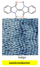 potential consequences for organic semiconductors, such as hydrogen bonding. That type of bonding is a relatively strong dipolar interaction present in many natural chemical systems, being responsible for the unique properties of water and the forces holding together DNA and RNA strands. Hydrogen bonding of so-called pi-conjugated molecules, where pi-pi interactions are strengthened by hydrogen bonds, yields highly ordered, high var epsilon (dielectric constant) organic films. The strong intermolecular interactions influence the dynamics of photogenerated excited states in such materials, which allow for many possibilities compared to disordered van der Waals bonded solids used in organic electronics today." potential consequences for organic semiconductors, such as hydrogen bonding. That type of bonding is a relatively strong dipolar interaction present in many natural chemical systems, being responsible for the unique properties of water and the forces holding together DNA and RNA strands. Hydrogen bonding of so-called pi-conjugated molecules, where pi-pi interactions are strengthened by hydrogen bonds, yields highly ordered, high var epsilon (dielectric constant) organic films. The strong intermolecular interactions influence the dynamics of photogenerated excited states in such materials, which allow for many possibilities compared to disordered van der Waals bonded solids used in organic electronics today." Source: Read the entire article...
|
|
Do You Have an Interesting Article to Share?
|
Interested in sharing the latest news in vacuum coating technology? Forward us a link to an article you want to share with the rest of the SVC readership to publications@svc.org. Purchase advertising space in this newsletter by contacting SVC at  svcinfo@svc.org. svcinfo@svc.org.
Society of Vacuum Coaters
71 Pinon Hill Place NE
Albuquerque, New Mexico 87122
505-856-7188
|
|
|
|
|