|
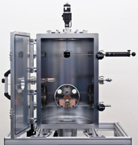
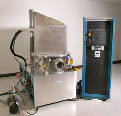
DLC Coating and Low Viscosity Oil Reduce Energy Losses Significantly
From "Hauzer for You", October 2011, by Dave Deerwald and Ruud Jacobs: "The motivation for the research has its roots in the EU regulations for CO2 emission and increasing oil prices. From 2012 on, due to EU regulations, car manufacturers have to pay an excess premium to compensate for every g/km deviation from the norm of 130 g/km. From 2012-2018 there is a gradient scale of calculation, but the amount of money involved can be really significant. Furthermore, in the last ten years the prices for gasoline and diesel increased more than forty percent. Energy losses occur in many parts of the vehicle.
In the Pegasus project concentration is on the rear axle, or more specifically on the hypoid pinion and the hypoid gear.
By introducing D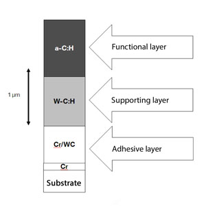 LC coating, an improvement of 1.5 percent in efficiency during boundary lubrication is achievable in the rear axle. A metal-free hydrogenated PVD/PECVD-DLC coating allows to reduce the friction, but also reduces wear. Oil splashing losses can be reduced by low-viscosity oil and conduction sheets, but leads to increased wear and friction at increasing loads and temperatures. However, since exactly here the coating has great potential, the combination of low viscosity oil and coating creates an excellent combination in friction reduction combined with low wear." LC coating, an improvement of 1.5 percent in efficiency during boundary lubrication is achievable in the rear axle. A metal-free hydrogenated PVD/PECVD-DLC coating allows to reduce the friction, but also reduces wear. Oil splashing losses can be reduced by low-viscosity oil and conduction sheets, but leads to increased wear and friction at increasing loads and temperatures. However, since exactly here the coating has great potential, the combination of low viscosity oil and coating creates an excellent combination in friction reduction combined with low wear."
Source:
Read the full article...
Hauzer Techno Coating: http://www.hauzertechnocoating.com/index/EN/DLC%20&%20Low%20Viscosity%20Oil/102/0/
Image: Hauzer Techno Coating
|
| |
|
Laser Patterning of Transparent Electrode Films: From Solar Panels Through High-End Displays
From Industrial Laser Solutions for Manufacturing, November 10, 2011, by Ralf Hellmann and Colin Moorhouse: "The availability of an expanded range of laser pulsewidths and wavelengths enables patterning of transparent conductive oxides to be optimized for applications as disparate as solar cells and OLED displays.
Thin films of transparent conductive oxides (TCOs) are used as  electrodes in applications where light must pass through the electrode, such as on the front side of certain solar cell types as well as in flat panel displays. Often, these conductive films must be scribed through to create a pattern of electrically isolated areas. Until now, the Q-switched nanosecond laser has dominated these applications, but the advent of newer displays, particularly those based on OLED technology, is creating a demand for even higher quality scribes. The authors have investigated the use of a picosecond laser for this purpose. This article presents the results of this testing which shows that picosecond lasers can deliver results which are superior to typical scribes created by ultraviolet nanosecond lasers." electrodes in applications where light must pass through the electrode, such as on the front side of certain solar cell types as well as in flat panel displays. Often, these conductive films must be scribed through to create a pattern of electrically isolated areas. Until now, the Q-switched nanosecond laser has dominated these applications, but the advent of newer displays, particularly those based on OLED technology, is creating a demand for even higher quality scribes. The authors have investigated the use of a picosecond laser for this purpose. This article presents the results of this testing which shows that picosecond lasers can deliver results which are superior to typical scribes created by ultraviolet nanosecond lasers."
Source:
Read the full article...
Industrial Laser Solutions/PennWell Corporation: http://www.industrial-lasers.com/articles/2011/11/laser-patterning-of-transparent-electrode-films-from-solar-panels-through-high-end-displays.html
Image: Ralf Hellmann and Colin Moorhouse
|
| |
|
Thin Film Module Manufacturers Directory 2011-2012 Unveiled by PV Insider
From PV Insider, October 26, 2011: "Researchers at PV Insider have completed work on the Thin Film Module Manufacturers Directory 2011-2012, as part of the launch of the 4th Annual Thin Film Solar Summit Europe. Hours of research has resulted in the general release of the Thin Film Module Manufacturers Directory 2011-2012, which shows a list of all the companies around the world involved in the manufacturing of thin film modules. The PDF splits the list down into separate thin film technologies, a-Si, CdTe and the CIS Family. Against each company you can see where they are headquartered, the type of technology they are involved in, and a link to the company website saving you the time of searching the internet.
The directory is free to download, and can be found here: www.pv-insider.com/thinfilmeu/directory.shtml
Source:
Read the full article...
PV Insider: Click here.
|
| |
|
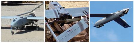
Specialized Thin Film Coatings for Unmanned Aircraft Systems
From NASA Tech Briefs, October 1, 2011, Eric W. Kurman, Deposition Sciences Inc.: "Unmanned aircraft systems (UAS) and their applications are experiencing rapid growth, especially in the area of remote sensing. Advances in propulsion; airframe materials; communications, command and control (C3) systems; cameras and detectors; and image processing are combining to continuously improve UAS capabilities. Most optical systems used in unmanned aircraft systems function over the visible (VIS) and near-infrared (NIR) wavelength ranges. Increasing in importance is multispectral or hyperspectral imaging which can combine information from VIS, NIR, mid-wave infrared (MWIR), and long-wave infrared (LWIR) wavelength regions to provide enhanced detection, such as chemical, vehicular, or terrain identification capabilities not available by the use of imaging alone. This article will cover some of the basics of optical thin film coatings as applied to electro-optical systems commonly used in unmanned systems."
Source:
Read the full article...
NASA Tech Briefs: http://www.techbriefs.com/component/content/article/11382
Images: NASA Tech Briefs
|
| |
|
The Evolution of Carbon Nanotubes during their Growth by PECVD
From Nanotechnology, September 12, 2011, by Hengzhi Wang, et al.: "During the growth of carbon nanotubes (CNTs) by plasma enhanced chemical vapor deposition (PECVD), plasma etching is the crucial factor that determines the growth mode and alignment of the CNTs. Focusing on a thin catalyst coating (5 nm Ni ), this study finds that the CNT growth by PECVD goes through three stages from randomly entangled (I-CNTs) to partially aligned (II-CNTs) to fully aligned (III-CNTs). The I-CNTs and II-CNTs are mostly etched away by the plasma as time goes by ending up with III-CNTs as the only product when growth time is long enough. However, with a thickness of the catalyst coating of 10 nm or more, neither I-CNTs nor II-CNTs are produced, but III-CNTs are the only type of CNTs grown during the whole growth process. During the growth of III-CNTs, the catalyst particles (Ni) stay on the tips of each of the aligned CNTs and act as a 'safety helmet' to protect the CNTs from plasma ion bombardment. On the other hand, it is also the plasma that limits the growth of III-CNTs, since the plasma eventually etches all the catalytic particles out and stops the growth." 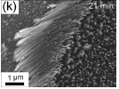 Source:
Read the full article...
Hengzhi Wang and Z.F. Ren, 2011 Nanotechnology 22 (October) 405601: http://iopscience.iop.org/0957-4484/22/40/405601/
Image: 1(k)
|
| |
|
University of Cincinnati Researcher Explores Possibility of Nanoscale Machining Facility
From www.azonano.com, November 1, 2011, by Cameron Chai: "University of Cincinnati's (UC) Micro and Nano Manufacturing Laboratory Director, Murali Sundaram is exploring the possibility of creating a cost -effective nano manufacturing facility where various small scale processes for machine substances can be carried out without requiring a highly clean laboratory environment.
Nano scale and micro scale manufacturing can be effectively used in applications such as coatings, measurement, micro electronics, biomedical, paintings and automotive industries.
The scientists' goal is to not only use processes at these scales but also to use them on a wide range of materials. Traditionally silicon's properties have been widely known as it is used in a majority of micro- electronic devices. However, some devices require other materials than silicon. The professor is currently investigating various alternative processes for different materials."
Source:
Read the full article...
www.azonano.com:
http://www.azonano.com/news.aspx?newsID=23684
|
| |
|
Thin Films: The Electronic Competition
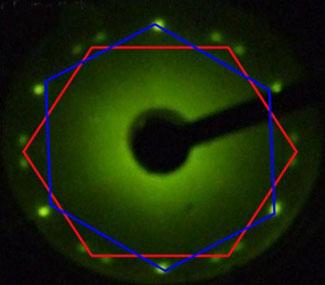
From Nanowerk News, October 31, 2011,: "The atom-by-atom growth of a crystalline film on a crystalline substrate, a process known as epitaxy, is employed in a wide range of applications to produce high-performance electronic interfaces and functionalities. Achieving the highest-quality interfaces generally involves matching the atomic lattice structures of the film and substrate. However, depending on the pairing of materials, achieving such lattice matching can be difficult, and the mechanisms governing growth in lattice-mismatched systems can be complex. Shu-Jung Tang and colleagues from National Tsing Hua University, the National Synchrotron Radiation Research Center and other institutions in Taiwan have now shown that the atomic structure of an epitaxial thin film is determined not only by atomic structural constraints, but also by electronic effects ("Electronic versus Lattice Match for Metal-Semiconductor Epitaxial Growth: Pb on Ge(111)"
Source:
Read the entire article...
www.nanowerk.com: http://www.nanowerk.com/news/newsid=23222.php
Image: Tokyo Institute of Technology
|
| | |
|
UNCD Thin Films Could Improve the Fabrication of Biosensors
From The Engineer, November 8, 2011, : "Scientists at Argonne National Laboratory's Center for Nanoscale Materials have successfully carved ultra-nanocrystalline diamond (UNCD) thin films into nanowires.
The development is likely to increase the material's functionality and provide potential improvements to the fabrication of biosensors.
UNCD thin films are a special form of diamond invented at ANL and are a subject of interest because of the material's ability to alter its electrical properties when the chemical bonding between grain boundaries is modified.
'It's a highly attractive carbon-based material with a range of applications in communications, medicine and defence,' said team leader Anirudha Sumant, a materials scientist at ANL.
A primary motive behind the team's studies, he said in a statement, is to understand the electrical transport properties of UNCD when it's fabricated into a nanowire geometry. Similarly, they wanted to see how these properties can be altered by changing chemical bonding at the grain boundary and by taking advantage of increased surface-to-volume ratio simultaneously."
Source: Click the link to read the full article. The Engineer: http://www.theengineer.co.uk/sectors/electronics/news/uncd-thin-films-could-improve-the-fabrication-of-biosensors/1010823.article
|
|
|
|
Viewpoint: Supercurrents Get Lean
From American Physical Society, November 7, 2011, by Chih-Kang Shih and Gregory A. Fiete, University of Texas at Austin: "For a material to transition into a superconducting state, two things have to happen: the electrons must form Cooper pairs (the carriers of superconducting current) and the pairs have to condense into a single phase. In low-dimensional materials, quantum fluctuations may disrupt the superconducting phase even when the Cooper pairs are able to form, leading to the question: How thin can a material be and still superconduct? Advances in synthesizing high-quality, ultrathin metal films have provided unprecedented opportunities to address this question. Experimental evidence suggests that superconductivity persists with a similar transition temperature, Tc, even in films that are only 1-2 atomic layers thick; however, these experiments have been based primarily on scanning tunneling spectroscopy, which detects the Cooper pairs, but not the existence of a macroscopic supercurrent. Whether an atomically thin film would also support supercurrents has therefore remained an open question. Now, in a paper appearing in Physical Review Letters, Takashi Uchihashi and co-workers at the National Institute for Materials Science in Tsukuba, Japan, provide a definite answer to this question by showing that robust supercurrents flow over macroscopic distances in an atomically thin metal film of indium. Their work is likely to push theorists and experimentalists to revisit the current understanding of low-dimensional superconductivity. "
 Source: Source:
Read the full article and paper, available free from American Physical Society.
Image: APS/Alan Stonebraker
|
|
|
|
A Single Polymer can be Used to Fabricate both Thin Film Transistors and Solar Cells
From Nanowerk News, November 9, 2011: " Polymers are the material of choice for making thin-film transistors and solar cells. They are also potentially suitable for manufacture using economical, high-throughput techniques, such as roll-to-roll and inkjet printing processes. However, transistors and solar cells have traditionally used different kinds of polymers, and this can severely complicate the fabrication process. Zhi-Kuan Chen at the A*STAR Institute of Materials Research and Engineering and co-workers have now developed a versatile polymer that is suitable for both kinds of devices ("A Versatile Low Bandgap Polymer for Air-Stable, High-Mobility Field-Effect Transistors and Efficient Polymer Solar Cells").
Polymers with high-charge mobilities are ideal to use in the manufacture of transistors. However, these materials are susceptible to having large energy bandgaps, which prevent them from absorbing portions of the solar spectrum. Such materials could severely hamper the energy conversion efficiency if made into solar cells."
Source:
Read the full article...
Nanowerk News: http://www.nanowerk.com/news/newsid=23336.php
|
|
|
|
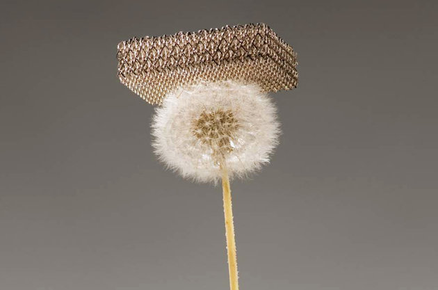
World's Lightest Solid Takes Inspiration from Eiffel Tower
From Yahoo News, November 18, 2011, by Charles Choi: "A metallic lattice of hair-thin pipes is now the lightest solid yet created - less dense than air, scientists revealed. The strategy used to create these intricate structures could lead to revolutionary materials of extraordinary strength and lightness, including ones made of diamond, researchers added.
Ultra-lightweight materials such as foams are widely used in thermal insulation and to dampen sounds, vibrations and shocks. They can also serve as scaffolds for battery electrodes and catalytic systems.
The very lightest substances in the world until now, aerogels, have the ethereal nickname "frozen smoke." They can reach densities of 1 milligram per cubic centimeter, making them less dense than air at room temperature and sea level.
The problem until now with low-density materials such as aerogels and metallic foams has been their random structures. For instance, aerogels are derived from gels whose liquid components were replaced with gas, leaving behind solid tangles of microscopic-bead necklaces. The chaotic architecture of these substances makes them much weaker than conventional forms of their parent material."
Source:
Read the full article...
Yahoo! News: http://news.yahoo.com/worlds-lightest-solid-takes-inspiration-eiffel-tower-134809070.html
Image: REUTERS/Dan Little/HRL Laboratories LLC
|
| |
|
Gallium Nitride Nanowires Achieve Crystalline Perfection
From SPIE, October 25, 2011, by Kristine Bertness, et al.:
"Gallium nitride (GaN) is a semiconductor material widely used for lighting and power transistor applications because of its abilities to emit UV and visible light and to tolerate high temperatures and voltages. [The] conventionally grown GaN films suffer from high defect densities arising from the merging of the crystal structure of the film with that of the wafer. The defects lead to weaker light emission, electrical signal noise, and early device failure.
 A number of crystal-growth 'tricks' reduce defect densities in ordinary GaN films or allow devices to be less sensitive to imperfections. Complete elimination of defects requires a more radical approach. Nanowire growth using a specific deposition method, molecular beam epitaxy (MBE), can achieve near-perfect crystal structure while retaining the semiconductor properties needed to make useful devices, as reviewed elsewhere." A number of crystal-growth 'tricks' reduce defect densities in ordinary GaN films or allow devices to be less sensitive to imperfections. Complete elimination of defects requires a more radical approach. Nanowire growth using a specific deposition method, molecular beam epitaxy (MBE), can achieve near-perfect crystal structure while retaining the semiconductor properties needed to make useful devices, as reviewed elsewhere."
Source:
Read the full article...
SPIE.org: http://spie.org/x57461.xml?highlight=x2400&ArticleID=x57461
Image: SPIE
|
| |
|
Predicting Plasma in Wafer Etch and Deposition via Quantum Mechanics
From ElectroIQ, November 7, 2011, Brent Walker, et al.: "Electron-molecule collisions drive technological plasmas. Electron energies and concentrations determine the gas phase chemistry, and therefore surface effects, in all plasma etch and deposition processes. Almost all micro-electronic devices now require dry and plasma processes to achieve the necessary surface detail, yet these plasma processes are still poorly understood.
TEL (Tokyo Electron Ltd.) and Quantemol Ltd. are collaborating on using the fully quantum mechanical R-matrix methods [1] to study the electron-molecule collision processes occurring in their plasma tools. The data provided by the R-matrix codes are used in reactor-scale models to simulate plasma behavior, allowing predictions of etch or deposition rates to be made.
The authors discuss the etching of silicon dioxide by fluorocarbons, and Ar/HBr etching in a microwave plasma source."
Source:
Click to read the full article
ElectroIQ.com: http://www.electroiq.com/articles/sst/2011/11/predicting-plasma-in-wafer-etch-and-deposition-via-quantum-mechanics.html
Image: Brent Walker, Quantemol Ltd., et al.
|
| |
|
Touchscreens Large and Small
From Hearst Electronic Products, October 26, 2011, by Binay Bajaj.: "Smartphones and tablet computers are omnipresent in today's society used by both businesses and consumers. ...First introduced on smaller devices several years ago, touchscreen-based devices are rapidly moving to larger formats as well.
However, moving from small screens and simple touch-enabled applications to a new paradigm where hands and fingers are the primary tools for interacting with computers is not going to be straightforward. Manufacturers must rethink the way touchscreens will be used and address new and more demanding requirements. Most important, the move to larger screen sizes has made a multiple touch capability essential. While a few finger strokes on today's 5-in. screens are sufficient, the minimum requirement for 12- and 40-in. devices is at least ten."
The article reviews capacitive and resistive touchscreen technologies and multitouch design factors.
Source:
Read the full article...
Hearst Electronic Products: http://www2.electronicproducts.com/Touchscreens_large_and_small-article-FAJH_Atmel_Nov2011-html.aspx
|
| |
Do You Have an Interesting Article to Share?

Interested in sharing the latest news in vacuum coating technology? Forward us a link to an article you want to share with the rest of the SVC readership to publications@svc.org. Purchase advertising space in this newsletterby contacting SVC at svcinfo@svc.org.
Society of Vacuum Coaters
71 Pinon Hill Place NE
Albuquerque, New Mexico 87122
505-856-7188
|
| |
|
VAT manufactures high quality vacuum valves for a variety of applications. Products include: gate, angle, fast-closing, transfer, pendulum, throttle, pressure control, all-metal and customized valves. See us at AVS: Booth 1405! Learn more.
Contact Us:
Phone: 781-935-1446
or 800-935-1446
E-Mail: US@vatvalve.com
|
| |

Roll Coating System
ULVAC's SPW-030 roll coating system is capable of processing 300 mm wide substrate compositions including thin-gauge metal rolls and polymeric materials for R&D and Pilot-scale production. Learn More.
ULVAC Technologies, Inc.
Visit Us Online
Tel: 1-978-686-7550
E-mail: sales@us.ulvac.com
|
| |
INFICON thin film deposition controllers, monitors and accessories, including customizable sensors and feedthroughs, offer features, function and value targeted to your application. View our catalog and contact us today!
INFICON
www.inficon.com
E-mail: reachus@inficon.com
|
|
|

Rebuilt Feedthroughs
Rigaku rebuilds ferrofluid feedthroughs for all leading manufacturers and offers a warranty on rebuilt units. Most parts are stocked in inventory for fast turnaround. Learn More.
Rigaku Vacuum Products
www.rigakuvacuum.com
E-mail: vacuum-info@rigaku.com
Phone: 603-890-6001
|
| |
Comdel's CB 5000 High Frequency RF Power Supply Now at
40.68 MHz and 60MHz
Comdel's CB 5000 high frequency reaches higher with 40.68 MHz and 60 MHz models. The CB5000 brings the highest power and frequency while keeping its small package and lightweight design. Learn more.
Comdel
11 Kondelin Road
Gloucester, MA 01930
Tel: 978-282-0620 or 800-468-3144
Fax: 978-282-4980
www.comdel.com
info@comdel.com
|
| |
|
MDC's Bundled Engineered Solutions
MDC offers virtually every component required for vacuum coating applications. With MDC's standard chamber line you have the advantage of bundling these high quality pieces together without hours or weeks of special engineering. More...
MDC
engineered process solutions
www.mdcvacuum.com
|
| |
|
From AR Coatings to Notch Filters, and from TCOs to DBRs, Evatec offers customized coating platforms and complete process solutions based on enhanced evaporation and sputter.
Phone: (603) 669-9656
www.evatecnet.com
E-Mail:infoNA@evatecnet.com
|
| |
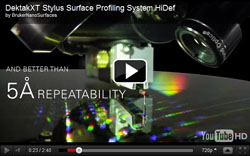
Measure Thin Film Deposition
with DektakXTTM
Bruker's new DektakXTTM stylus profiler monitors thin film deposition and etch systems with the industry's best measurement repeatability (<5Å). Find out how to better control your thin film process development faster, easier and more accurately. Learn More.
Bruker Corporation
520-741-1044
productinfo@bruker-nano.com
|
| |
|
 Rectangular Port Vacuum Valves Rectangular Port Vacuum Valves
Ports to 200 X 1400 mm; 8 X 55 inch.
Aluminum, Steel or Stainless Steel.
(RoHS) 2002/95/EC Compliant.
Auto Close or Open on Power Fail.
NW and ISO Gauge & Roughing Ports.
Vacuum Research Corporation Phone: 800/426-9340
Web: www.vacuumresearch.com
E-Mail: vrc@vacuumresearch.com
|
| |
|
Dynavac's Diamond-Like Carbon Deposition System produces infrared and anti-reflection coatings for commercial and military applications on substrates up to 24" diameter.
www.dynavac.com
Telephone: 781-740-8600
E-Mail: sales@dynavac.com |
| |
|

Evans Analytical Group (EAG) is the leading global provider of high quality surface analysis and materials characterization services to the films and coatings industry.
Evans Analytical Group
1.800.366.3867
|
| |
|

Veeco provides RF Linear Ion Sources for medium and large scale substrates featuring a broad power range and patented technology that provides reliability and performance.
To Learn More Visit:
www.veeco.com
970-221-1807
|
| |
|

Solid Sealing Technology designs and manufactures hermetic assemblies using metalizing, brazing and glass-ceramic sealing including standard and custom Feedthroughs/Connectors for extreme environments and UHV.
Contact:
Ph: 518-874-3600
Fax: 518-874-3610
info@solidsealing.com
|
| |
Thin-Films Research is prepared to meet your custom thin-film coating requirements. Using state-of-the-art equipment and over 40 years of experience, Thin-Films Research offers technology for the electro-optics, semiconductors, sensors & medical electronic industries. Learn More
Thin-Films Research, Inc.
270 Littleton Road
Westford, MA 01886
Phone: 978-692-9530
Fax: 978-692-9531
E-Mail: sales@thinfilmsresearch.com |
| |
|
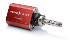
Intelligent RGA
The PrismaPlus™ mass spectrometer delivers qualitative and quantitative gas analysis and leak detection. It provides precise and stable results to 300 amu with a detection limit of 1x10-14 mbar. Learn More.
Pfeiffer Vacuum, Inc.
24 Trafalgar Square
Nashua, NH 03063-1988
Phone: 603-578-6500
www.pfeiffer-vacuum.com
prismaplus@pfeiffer-vacuum.com
|
| |
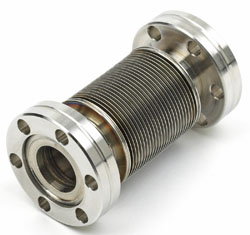
BellowsTech's proprietary diaphragm manufacturing process creates high yield, high strength bellows by ensuring the diaphragms are extremely concentric, and the metal is not stressed during its formation.
Learn more.
|
| |
EQP Mass and Energy Analyser for Plasma Diagnostics
- Plasma ion analyser for +ve and -ve ion analysis
- Neutrals and neutral radical detection
- For correlation of plasma parameters with film quality Learn More
E-mail address: info@hiden.co.uk
Phone: +44 [0] 1925 445225 (UK)
or [1] 734 542 6666 (USA)
Website:www.HidenAnalytical.com
|
| |

April 28 - May 3, 2012
Santa Clara, California
Technical Program
Exhibit
Education
Networking
Learn More...
|
|
FRIDAY, DECEMBER 9
Practical Aspects of Plasma Modification of Polymer Materials and Plasma Web Treatment
Instructor: Jeremy M. Grace
December 9, 2011 11 am - 2 pm EST
Course Description and Pricing
Registration is Open
On-Demand Webinar Available Sputter DepositionInstructor: David Glocker Originally Presented Sept. 14. 2011Available until December 15, 2011
|
| |
|