|
New Probe to Uncover Mechanisms Key to Fusion Reactor Walls
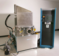
From Purdue University, University News Service, August 25, 2011: "A new tool developed by nuclear engineers at Purdue University will be hitched to an exp erimental fusion reactor at Princeton University to learn precisely what happens when extremely hot plasmas touch and interact with the inner surface of the reactor. erimental fusion reactor at Princeton University to learn precisely what happens when extremely hot plasmas touch and interact with the inner surface of the reactor.
The work is aimed at understanding plasma-wall interactions to help develop coatings or materials capable of withstanding the grueling conditions inside fusion reactors, known as tokamaks. The machines house a magnetic field to confine a donut-shaped plasma of deuterium, an isotope of hydrogen."
The research "will provide information about how the coating materials evolve under plasma conditions and how the interaction correlates with changes in the plasma itself."
Source:
Click on the link to read the full article
Purdue University: http://www.purdue.edu/newsroom/research/2011/110825AllainFusion.html
Image: Emil Venere and Jean Paul Allain, Purdue University
|
| |
|
At the Forefront of Plasma-Surface Interaction
From CNRS International Magazine (French National Center for Scientific Research), July 2011, p. 41, by Elaine Cobbe: "Researchers from France and Luxembourg join forces to advance knowledge in plasma physics. European Associated Laboratory (LEA) LIPES, was created in January 2010.
For its initial four-year term (2010-2013), this "laboratory without walls" will work on studying the interactions between a plasma source a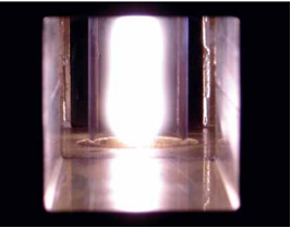 nd the topmost surface of various materials. The scientists will focus on "building" the top surface, from the single plasma species deposited on the material up to the complete monolayer. In this way, they hope to better understand the behavior of any isolated species as it touches the surface." nd the topmost surface of various materials. The scientists will focus on "building" the top surface, from the single plasma species deposited on the material up to the complete monolayer. In this way, they hope to better understand the behavior of any isolated species as it touches the surface."
Source:
Click on the link to read the full article
CNRS International Magazine: http://www.cnrs.fr/fr/pdf/cim/22/index.html#/40/
Image: LIPES |
|
|
|
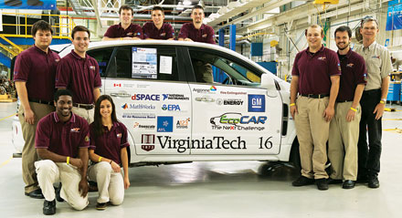
DOE Plans Shift in R&D Direction
From Chemical & Engineering News, Oct. 3, 2011, by Jeff Johnson: ""The Department of Energymust reshuffle its research direction, according to an expert panel created to guide the agency's research needs over the next four years. In particular, the panel recommends a shift toward transportation-related R&D and away from aid to stationary sources of clean electricity.
Energy Secretary Steven Chu and Under Secretary for Science Steven E. Koonin rolled out the panel's report, the "Quadrennial Technology Review," on Sept. 27 at a briefing attended by a highly supportive and receptive audience of scientists. The first-of-its-kind review grew from recommendations of the President's Council of Advisors on Science & Technology, which urged DOE to better prioritize energy R&D. The biggest proposed change in research direction, according to DOE, is a shift to electric vehicles."
Source:
Click on the link to read the full article
Chemical & Engineering News: http://cen.acs.org/articles/89/i40/DOE-Plans-Shift-RD-Direction.html
Image: DOE Advanced Vehicle Technology Competitions
|
| |
|
3Q 2011 Global Cleantech Venture Investments up 12% from Previous Quarter
From Cleantech Group, Oct. 5, 2011: "Cleantech Group™, a global research firm focused on cleantech innovation, released preliminary 3Q 2011 results for clean technology venture investments around the globe, totaling $2.23 billion across 189 deals. Measured by dollars invested, cleantech venture investment grew 12 percent compared to the previous quarter ($1.98 billion) and was also 23 percent higher than 3Q10 ($1.81 billion).
'While financing remains constrained, it's great to see growth in venture activity,' said Sheeraz Haji, CEO of Cleantech Group. 'Energy Storage emerged as our top sector, indicating continued strong interest in advanced technologies for grid-storage as well as for electric vehicles. Global enterprises continue to invest aggressively into cleantech.'
For the first time, energy storage was the leading sector by amount invested ($514 million), followed by solar ($350 million) and energy efficiency ($223 million). Energy efficiency was the most popular sector measured by number of deals, ahead of solar and energy storage. North America accounted for 76 percent of the total amount invested, Asia Pacific for 14 percent and Europe & Israel for 10 percent."
Source:
Click on the link to read the full article.
Cleantech Group: http://www.cleantech.com/2011/10/05/3q-2011-global-cleantech-venture-investment-up-12-percent-from-previous-quarter/
|
| |
|
Experiments Help Refine Thin-Film Solar Cells
From Oak Ridge National Laboratory, Sept. 1, 2011, by Deborah Counce: "Neutron scattering experiments conducted at Oak Ridge National Laboratory are helping solar cell makers obtain the hard data they need to refine their materials and manufacturing processes.
Recent studies of polymer-based solar cells at ORNL's Spallation Neutron Source and High Flux Isotope Reactor revealed important details about their molecular structure and showed that annealing (heat treating) the devices improves their power conversion efficiency. The experiments showed that annealing solar cells appropriately as they are fabricated improves their efficiency by more than 20 percent compared to films that aren't annealed.  'We are trying to use mixtures of photoactive polymers to absorb light over a broad wavelength range to improve efficiency,' said principal investigator Thomas Russell of University of Massachusetts-Amherst. Haiyun Lu of U-Mass and Bulent Akgun of the NIST Center for Neutron Research and the University of Maryland are co-investigators. Studies such as this one are key to improving the performance of polymer-based solar cells so that they can compete in the marketplace."
Source:
Click the link to read the full article:
Oak Ridge National Laboratory: http://www.ornl.gov/info/features/get_feature.cfm?FeatureNumber=f20110901-01
Image: Kent Fiel, Creative Commons
|
| |
|
Structural Efficiency Boost Heralds Third-Generation Solar Cells
From SPIE.org, October 11, 2011, by Navab Singh et al.: "The majority of solar cells are made of crystalline silicon-a material used for electronic circuits-that has a high production cost ($1.80 per peak watt). By contrast, low-grade silicon is a cheaper alternative that is widely used in thin-film solar cells. However, poor absorption of light and poor collection of resulting electric charge carriers result in a 50% reduction in efficiency compared to crystalline silicon.
 Poor reflection control (light not entering the film) and poor light trapping (light not being absorbed once inside) reduce light absorption. Defects inside the films also annihilate charge carriers before they can contribute to the electrical output, and so reduce the collection efficiency. We therefore added periodic vertical nanostructures to improve thin-film solar cells' reflection control, light trapping behavior, and collection efficiency." Poor reflection control (light not entering the film) and poor light trapping (light not being absorbed once inside) reduce light absorption. Defects inside the films also annihilate charge carriers before they can contribute to the electrical output, and so reduce the collection efficiency. We therefore added periodic vertical nanostructures to improve thin-film solar cells' reflection control, light trapping behavior, and collection efficiency." Source:
Click the link to read the full article
SPIE.org: http://spie.org/x57208.xml?ArticleID=x57208
Image: SPIE
|
| |
|
Moving Away from Silicon Technology
From Nanowerk.com, October 3, 2011: "Silicon, the conventional semiconductor used to build up electronics, is processed at very high temperature -over one thousand Celsius degrees- and it is difficult to recycle. With the aim of facilitating the sustainable and competitive manufacture of new displays with low-cost technology, scientists of the European project MULTIFLEOXIDES have developed new ceramic thin films containing amorphous or nano-structured oxides processed at low temperature to be used as transparent materials, conducting, semiconducting or insulating components in rigid and flexible electronic devices.
'"The challenge is that we use zinc, which is a ceramic good-behaviour material, with gallium and indium and mix it within oxide to make new materials with electronic performances as good as silicon, something that was never tried before' says Rodrigo Martins, director of CEMOP (Center of Excellence in Microelectronics Optoelectronics and Processes) at the Portuguese University-Enterprise association UNINOVA (Institute for the Development of New Technologies), president of the European Materials Research Society and coordinator of the MULTIFLEOXIDES project."
Source: Click the link to read the full article:
Nanowerk.com: http://www.nanowerk.com/news/newsid=22938.php
|
| |
|
Vacuum Coating Processing System for CIGS Cells Unveiled
From Solarserver.com, Oct. 18, 2011: "Singulus Technologies AG (Kahl am Main, Germany) unveiled a new processing system for vacuum coating copper indium gallium diselenide (CIGS) thin-film solar photovoltaic (PV) cells.
The company also reported its first order for the system to an un-named customer. Singulus states that the main advantage of the system is that it can be used for the vertical vacuum-based coating of glass substrates.
The tool is a response to demand for tools that increase the efficiency of CIGS cells while cutting production costs. The company also notes that production of the tool gives it a new field of operations in the market for thin-film PV, in addition to its wet-processing and selenization systems for CIGS cells.
Source: Click on the link to read the entire article:
Solarserver.com: http://www.solarserver.com/solar-magazine/solar-news/current/2011/kw42/pv-manufacturing-equipment-singulus-unveils-vacuum-coating-processing-system-for-cigs-cells.html
Image: Singulus
|
| | |
|
Polymer Characterization 'Tweezers' Turn Nobel Theory into Benchtop Tool
From EurekAlert!, Oct. 19, 2011: "Researchers at UC Santa Barbara have developed a new and highly efficient way to characterize the structure of polymers at the nanoscale - effectively designing a routine analytical tool that could be used by industries that rely on polymer science to innovate new products, from drug delivery gels to renewable bio-materials.
Professor Omar Saleh and graduate student Andrew Dittmore of the UCSB Materials department have successfully measured the structure and other critical parameters of a long, string-like polymer molecule - polyethylene glycol, or PEG - by stretching it with an instrument called magnetic tweezers.
'We attach one end of the PEG molecule to a surface, and the other to a tiny magnetic bead, then pull on the bead by applying a magnetic field,' explained Saleh. 'The significance is that we're able to perform the elastic measurements - force vs. length measurement - to see aspects of polymer structure that are hard to see in any other way, and we can do it within minutes on a benchtop apparatus.'"
Source: Click the link to read the full article.
EurekAlert.org: http://www.eurekalert.org/pub_releases/2011-10/uoc--pc101711.php
|
|
|
|
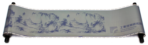
Green Technologies Receive 2011 R&D 100 Awards
From MarketWatch.com, Oct 13, 2011: "ITRI (Industrial Technology Research Institute), Taiwan's largest and one of the world's leading high-tech research and development institutions, will accept two 2011 R&D 100 Awards this evening in Orlando, Fla. for its innovative, breakthrough technologies: i2Re-Paper(TM) (Materials Sciences category), the first green re-writable and re-usable electronic paper technology to provide an environmentally friendly recyclable print medium alternative to traditional paper and ink consumption, and HyTAC (TM) (Thin-film and Vacuum Technologies category), the world's first environmentally friendly polarizer protective film for LCD displays used in many consumer electronics.
i2R e-Paper's special energy-conserving display technology -- a flexible cholesteric liquid crystal panel -- requires only heat to store and transmit images, without using expensive inks. i2R e-Paper delivers a 300 dpi high-resolution and 16 grey level image that remains crisp until users decide to re-write the e-paper. It is both eco-friendly and re-writable close to 300 times"
Source: Click the link to read the full article.
Image: ITRI
|
|
|
|
NASA's Webb Telescope Completes Mirror-Coating Milestone
From NASA.gov, Sept. 13, 2011: "NASA's James Webb Space Telescope has reached a major milestone in its development. The mirrors that will fly aboard the telescope have completed the coating process at Quantum Coating Inc. in Moorestown, N.J.
The Webb telescope has 21 mirrors, with 18 mirror segments working together as one large 21.3-foot (6.5-meter) primary mirror. The mirror segments are made of beryllium, which was selected for its stiffness, light weight and stability at cryogenic temperatures. Bare beryllium is not very reflective of near-infrared light, so each mirror is coated with about 0.12 ounce of gold.
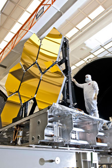
The Webb telescope is the world's next-generation space observatory and successor to the Hubble Space Telescope. The most powerful space telescope ever built, the Webb telescope will provide images of the first galaxies ever formed, and explore planets around distant stars. It is a joint project of NASA, the European Space Agency and the Canadian Space Agency."
Source: Click the link to read the full article.
NASA.gov: http://www.nasa.gov/topics/technology/features/webb-mirror-coating.html
Image: NASA/Chris Gunn
|
|
|
|
Metamaterials: Photonic Sleight of Hand
From Photonics Spectra, September 2011, by Marie Freebody: "The field of metamaterials is barely 10 years old. First conceived in 2000 by Sir John Pendry at Imperial College London, metamaterials relied in the early days on advances in nanotechnology to build tiny structures such as metallic rings or wires smaller than the wavelength of light. These nanostructures modify the electromagnetic properties of the metamaterial, sometimes creating seemingly impossible optical effects.
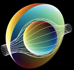
In the optical regime, the visionary applications such as enhanced photovoltaic light collection, biosensing, perfect imaging, all-optical memories and, of course, invisibility cloaks are expected to have the highest and most wide-ranging impact.
Although the basic building blocks and enabled functionalities of these extraordinary media have (at optical wavelengths) been created and experimentally demonstrated, bringing optical metamaterials out of the laboratory remains a tall order, said professor Ortwin Hess, the Leverhulme Chair in Metamaterials at Imperial College London."
Source:
Click to read the full article
Photonics Media: http://www.photonics.com/Article.aspx?AID=48167
Image: John Pendry, Imperial College London
|
| |
|
Microexplosion Reveals New Superdense Aluminum
From Advanced Materials & Processes, Oct. 2011, page 6:
"A research team including Arturas Valionis of SLAC National Accelerator Laboratory, Stanford University, Calif., blasted tiny 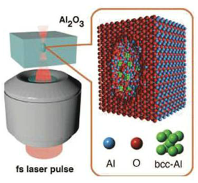 bits of sapphire with a new table-top laser device that penetrates crystals and sets off microexplosions inside them, creating powerful shock waves that compress the surrounding material. Under extreme conditions, warm dense matter forms, the state of matter between a solid and a plasma. Because sapphire is a form of aluminum oxide, or alumina, researchers expected to find evidence of various phases of high-pressure alumina inside the get. Instead, they observed minuscule amounts of a stable, highly compressed form of elemental body-centered-cubic aluminum." bits of sapphire with a new table-top laser device that penetrates crystals and sets off microexplosions inside them, creating powerful shock waves that compress the surrounding material. Under extreme conditions, warm dense matter forms, the state of matter between a solid and a plasma. Because sapphire is a form of aluminum oxide, or alumina, researchers expected to find evidence of various phases of high-pressure alumina inside the get. Instead, they observed minuscule amounts of a stable, highly compressed form of elemental body-centered-cubic aluminum."
Source:
Click to read view the October 2011 issue. Article is found on page 6.
Advanced Materials & Processes:
http://amp.asminternational.org/
Image: SLAC/Stanford
|
| |
|
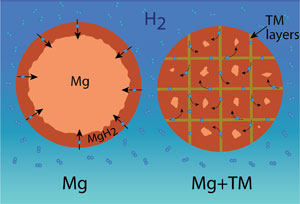
Iron 'Veins' are Secret of Promising New Hydrogen Storage Material
From NIST TechBeat, August 30, 2011: "With a nod to biology, scientists at the National Institute of Standards and Technology (NIST) have a new approach to the problem of safely storing hydrogen in future fuel-cell-powered cars. Their idea: molecular scale "veins" of iron permeating grains of magnesium like a network of capillaries. The iron veins may transform magnesium from a promising candidate for hydrogen storage into a real-world winner.
Hydrogen has been touted as a clean and efficient alternative to gasoline, but it has one big drawback: the lack of a safe, fast way to store it onboard a vehicle. According to NIST materials scientist Leo Bendersky, iron-veined magnesium could overcome this hurdle. The combination of lightweight magnesium laced with iron could rapidly absorb-and just as importantly, rapidly release-sufficient quantities of hydrogen so that grains made from the two metals could form the fuel tank for hydrogen-powered vehicles."
Source:
Click to read the full article
NIST Tech Beat: http://www.nist.gov/mml/metallurgy/hydrogen-083011.cfm
Image: NIST
|
| |
Do You Have an Interesting Article to Share?

Interested in sharing the latest news in vacuum coating technology? Forward us a link to an article you want to share with the rest of the SVC readership to publications@svc.org. Purchase advertising space in this newsletterby contacting SVC at svcinfo@svc.org.
Society of Vacuum Coaters
71 Pinon Hill Place NE
Albuquerque, New Mexico 87122
505-856-7188
|
| |
|
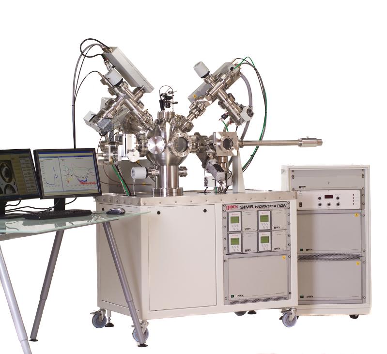
SIMS Workstation
A high performance SIMS instrument for:
- Thin film depth profiling
- Surface imaging
- Features new high sensitivity sputtered neutrals detection mode for quantitative analysis.
Learn more.
E-mail address: info@hiden.co.uk
Phone: +44 [0] 1925 445225 (UK)
or [1] 734 542 6666 (USA)
Website: www.HidenAnalytical.com
|
| |
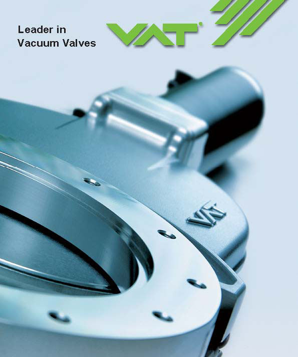
VAT manufactures high quality vacuum valves for a variety of applications. Products include: gate, angle, fast-closing, transfer, pendulum, throttle, pressure control, all-metal and customized valves. See us at AVS: Booth 1405! Learn more.
Contact Us:
Phone: 781-935-1446
or 800-935-1446
E-Mail: US@vatvalve.com
|
| |

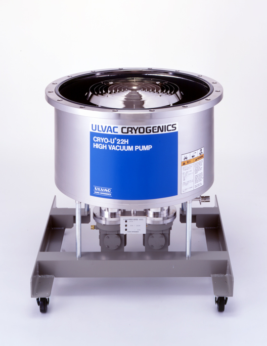
Large Cryo Pumps
ULVAC's reliable large cryogenic pumps deliver high refrigeration power, maximum pumping speed and capacity at 20", 22" and 30". Specialty versions are available including low vibration and corrosion proof. Learn More.
ULVAC Technologies, Inc.
Visit Us Online
Tel: 1-978-686-7550
E-mail: sales@us.ulvac.com
|
| |
INFICON thin film deposition controllers, monitors and accessories, including customizable sensors and feedthroughs, offer features, function and value targeted to your application. View our catalog and contact us today!
INFICON
www.inficon.com
E-mail: reachus@inficon.com
|
|
|
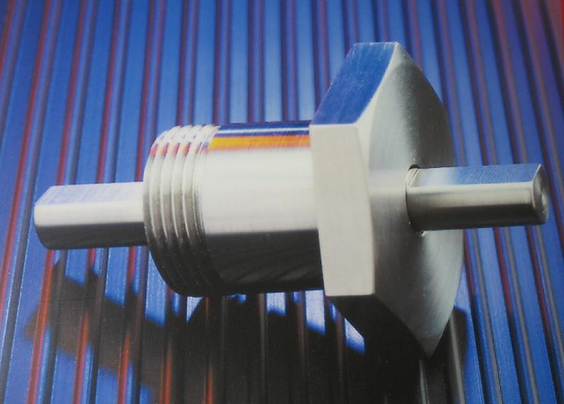
Rotary Motion Feedthroughs
Rigaku offers a full range of feedthroughs, including low cost SuperseaL, hollow shaft, solid shaft, motorized, UHV, custom designs and competitive direct replacements.
Learn More
Rigaku Vacuum Products
www.rigakuvacuum.com
E-mail: vacuum-info@rigaku.com
Phone: 603-890-6001
|
| |
Comdel's Matching Networks Will Keep You In Tune
Comdel's Matching Networks are engineered with PROTRAK, a high-speed tuning algorithm that gradually slows the system as it approaches the tuning point, allowing a precise match even in high "Q" loads. Learn more.
Comdel
11 Kondelin Road
Gloucester, MA 01930
Tel: 978-282-0620 or 800-468-3144
Fax: 978-282-4980
www.comdel.com
info@comdel.com
|
| |
|
MDC's Bundled Engineered Solutions
MDC offers virtually every component required for vacuum coating applications. With MDC's standard chamber line you have the advantage of bundling these high quality pieces together without hours or weeks of special engineering. More...
MDC
engineered process solutions
www.mdcvacuum.com
|
| |
|
From AR Coatings to Notch Filters, and from TCOs to DBRs, Evatec offers customized coating platforms and complete process solutions based on enhanced evaporation and sputter.
Phone: (603) 669-9656
www.evatecnet.com
E-Mail:infoNA@evatecnet.com
|
| |
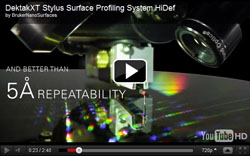
Measure Thin Film Deposition
with DektakXTTM
Bruker's new DektakXTTM stylus profiler monitors thin film deposition and etch systems with the industry's best measurement repeatability (<5Å). Find out how to better control your thin film process development faster, easier and more accurately. Learn More.
Bruker Corporation
520-741-1044
productinfo@bruker-nano.com
|
| |
|
 Rectangular Port Vacuum Valves Rectangular Port Vacuum Valves
Ports to 200 X 1400 mm; 8 X 55 inch.
Aluminum, Steel or Stainless Steel.
(RoHS) 2002/95/EC Compliant.
Auto Close or Open on Power Fail.
NW and ISO Gauge & Roughing Ports.
Vacuum Research Corporation Phone: 800/426-9340
Web: www.vacuumresearch.com
E-Mail: vrc@vacuumresearch.com
|
| |
|
Dynavac's Diamond-Like Carbon Deposition System produces infrared and anti-reflection coatings for commercial and military applications on substrates up to 24" diameter.
www.dynavac.com
Telephone: 781-740-8600
E-Mail: sales@dynavac.com |
| |
|

Evans Analytical Group (EAG) is the leading global provider of high quality surface analysis and materials characterization services to the films and coatings industry.
Evans Analytical Group
1.800.366.3867
|
| |
|

Veeco provides RF Linear Ion Sources for medium and large scale substrates featuring a broad power range and patented technology that provides reliability and performance.
To Learn More Visit:
www.veeco.com
970-221-1807
|
| |
|

Solid Sealing Technology designs and manufactures hermetic assemblies using metalizing, brazing and glass-ceramic sealing including standard and custom Feedthroughs/Connectors for extreme environments and UHV.
Contact:
Ph: 518-874-3600
Fax: 518-874-3610
info@solidsealing.com
|
| |

Nanovea manufactures Profilometers, Mechanical Testers & Tribometers to combine the most advanced testing capabilities in the industry. And unlike other manufacturers, Nanovea also provides Laboratory Services.
Learn More
www.nanovea.com
E-Mail: info@nanovea.com
Phone: 949-461-9292 |
| |

Thin-Films Research is prepared to meet your custom thin-film coating requirements. Using state-of-the-art equipment and over 40 years of experience, Thin-Films Research offers technology for the electro-optics, semiconductors, sensors & medical electronic industries. Learn More
Thin-Films Research, Inc.
270 Littleton Road
Westford, MA 01886
Phone: 978-692-9530
Fax: 978-692-9531
E-Mail: sales@thinfilmsresearch.com |
| |
|

Custom Cubical Vacuum Chambers
Pfeiffer Vacuum offers two week lead time and pricing starting at $5900 for 12" and $7400 for 20" custom cubical vacuum chambers. Other chamber sizes and shapes are also available.
Pfeiffer Vacuum, Inc.
24 Trafalgar Square
Nashua, NH 03063-1988
Phone: 603-578-6500
Web site: www.trinos.com
hardware@pfeiffer-vacuum.com
|
| |
Edge-Welded Bellows Technology
Edge welded bellows are manufactured by welding stamped, metal diaphragms into a long, flexible assembly. Learn about the manufacturing process used, and how BellowsTech can design your solution. Learn More.
BellowsTech, LLC
Phone: 386-615-7530
www.bellowstech.com
Email: bellows@bellowstech.com
|
| |

April 28 - May 3, 2012
Santa Clara, California
Technical Program
Exhibit
Education
Networking
Learn More...
|
|
Next Live Webinar
Practical Aspects of Plasma Modification of Polymer Materials and Plasma Web Treatment
Instructor: Jeremy M. Grace
December 9, 2011 11 am - 2 pm EST
Course Description and Pricing
Registration is Open
On-Demand Webinar Available Sputter DepositionInstructor: David Glocker Originally Presented Sept. 14. 2011Available until December 15, 2011
|
| |
|