|
SUNPATH: DOE to Invest $50 Million to Advance Solar Manufacturing, Achieve SunShot Goal
From U.S. Department of Energy, EERE News, August 2, 2011: "U.S. Energy Secretary Steven Chu today announced a $50 million investment over two years for the SUNPATH program, aimed to help the nation reclaim its competitive edge in solar manufacturing. SUNPATH, which stands for Scaling Up Nascent PV At Home, represents the second solar Photovoltaic Manufacturing Initiative (PVMI) supporting the Department of Energy's SunShot Initiative.
SUNPATH seeks to increase domestic manufacturi ng through investments that have sustainable, competitive cost and performance advantages. SUNPATH will help companies with pilot-scale commercial production scale up their manufacturing capabilities, enabling them to overcome a funding gap that often curtails domestic business at a critical stage. By bridging this gap, SUNPATH will help ensure that innovative, low-cost solar technologies are manufactured in the United States. ng through investments that have sustainable, competitive cost and performance advantages. SUNPATH will help companies with pilot-scale commercial production scale up their manufacturing capabilities, enabling them to overcome a funding gap that often curtails domestic business at a critical stage. By bridging this gap, SUNPATH will help ensure that innovative, low-cost solar technologies are manufactured in the United States.
The Department of Energy is seeking applicants with industrial-scale demonstrations of PV modules, cells, or substrates that offer lower-cost solutions in line with the SunShot goal. Applications are due by October 28, 2011."
Source:
Click on the link to read the full article
EERE News, U.S. Department of Energy: http://apps1.eere.energy.gov/news/daily.cfm/hp_news_id=314
Learn More About the SunShot Initiative: http://www1.eere.energy.gov/solar/sunshot/
Image: DOE/Energy Efficiency and Renewable Energy
|
| |
|
Turnkey Manufacturing 2.0: Manufacturers Move Away From Traditional Fab Models
From Solar Industry Magazine, August 2011, pp. 38-40, by Gail Kalinoski: World-wide popularity in purchasing traditional turnkey PV module production equipment has decreased in recent years. Turnkey customers are those requiring fast start-up or fast expansion. Others lacking technical manufacturing knowledge use turn-key systems to get into the market quickly and gain experience
The equipment model is changing to more custom processes. For example, Spire Corporation is experiencing increased demand for "partial" turnkey lines for post-lamination module production. In addition, Finlay Coleville, analyst at Solarbuzz market research firm, points out that business is shifting from large-scale solar module manufacturers to selling tooling, "including software and process control", for factories. There are other module manufacturers with specialized designs where perhaps one piece of standard equipment is purchased or all production equipment is designed in-house. The equipment needs are changing dramatically.
Source:
Click on the link to access the August 2011 issue:
Solar Industry Magazine, pp. 38-40: http://www.solarindustrymag.com/editorial/current.php
Spire Corporation: http://www.spirecorp.com/spire-solar/fast-line-Post-Lamination-PV-Module-Assembly-and-Testing/index.php |
|
|
|
I-Corps: To Strengthen the Impact of Scientific Discoveries
From National Science Foundation, July 28, 2011: "The National Science Foundation (NSF) announced a new effort to help develop scientific and engineering discoveries into useful technologies, products and processes.
The NSF Innovation Corps (I-Corps) program, a public-private partnership, will connect NSF-funded scientific research with the technological, entrepreneurial and business communities to help create a stronger national ecosystem for innovation that couples scientific discovery with technology development and societal needs.
'The United States has a long history of investing in--and deploying--technological advances derived from a foundation of basic research,' says NSF Director Subra Suresh. With the awards, the I-Corps initiative will strategically identify nascent concepts and leverage NSF's investment in basic research for technology innovation. The I-Corps program will initially support up to 100 projects per year, at $50,000 a project. Proposals are due September 9, 2011 and Awards will be announced on September 30, 2011."
Source:
Click on the link to read the full article
NSF: Learn More
Read the I-Corps Fact Sheet: http://www.nsf.gov/news/newsmedia/i-corps/factsheet.pdf
Image: National Science Foundation
|
| |
|
U.S. Army Establishes Task Force for Large-Scale Renewable Energy Projects
From U.S. Department of Defense, August 10, 2011:
"John M. McHugh, Secretary of the Army, announced today the establishment of the Energy Initiatives Office (EIO) Task Force at the GovEnergy Conference in Cincinnati, Ohio. The EIO Task Force is part of the Office of the Assistant Secretary of the Army for Installations, Energy and Environment, and will serve as the central managing office for the development of large-scale Army renewable energy projects. The EIO Task Force will be fully operational by Sept. 15, 2011.
The new EIO Task Force is integral to the Army addressing rising energy security challenges, escalating fuel prices, and stricter federal mandates. McHugh said, 'To meet a goal of 25 percent renewable energy by 2025, the Army must use every opportunity to be energy efficient and draw power from alternative and/or renewable energy sources.'
The scale of renewable energy production the Army needs in order to provide enhanced energy security is estimated to require investment up to $7.1 billion over the next 10 years. This level of investment is expected to generate 2.1 million megawatt hours of power annually for the Army."
Source:
Click on the link to read the full article.
U.S. Department of Defense: http://www.defense.gov/releases/release.aspx?releaseid=14726
|
| |
|
PS-PVD Processing Varies Coating Architecture with Processing Parameters
From Advanced Materials & Processes Magazine, August 2011, by Brian Harder, Ph.D., NASA Glenn Research Center: "The next generation of protective coatings for turbine engine materials will require a deposition method with rapid processing speed, materials flexibility, and the capability to create thin coatings with unique microstructures. Bridging the gap between APS (air plasma spray) and EB-PVD (electron beam-physical vapor deposition) methods, PS-PVD (plasma spray-physical vapor deposition) offers the enhanced capabilities required for coating advanced engine components. PS-PVD technology, developed by Sulzer-Metco (Wohlen, Switzerland) is a unique type of low pressure plasma spray, which deposits coatings in a controlled environment at a reduced pressure ranging from 70-1300 Pa.
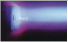 A wide range of microstructures, feedstock, flexibility, and speed of coating deposition make this an attractive processing technique for a variety of industries. Wear or electrically resistive coatings, diffusion barrier layers, ion-transport layers for fuel cell components, or gas-sensing membranes could benefit from this type of processing." A wide range of microstructures, feedstock, flexibility, and speed of coating deposition make this an attractive processing technique for a variety of industries. Wear or electrically resistive coatings, diffusion barrier layers, ion-transport layers for fuel cell components, or gas-sensing membranes could benefit from this type of processing."
Source:
Click on the link to the ASM website. Click the "Open Document" Button to read the entire article on pp.49-51:
Advanced Materials & Processes: iTSSe Insert
Image: NASA Glen Research Center
|
| |
|
Making Films One Layer at a Time
From Chemical & Engineering News, August 1, 2011, by Mitch Jacoby: " ALD's reach extends far beyond semiconductors, according to Jill Becker, chief executive officer and founder of Cambridge NanoTech, a manufacturer of ALD research and industrial equipment based in Cambridge, Mass. With its ability to apply perfect films to complex three-dimensional objects, ALD is quickly making headway into lighting and flexible-display technologies; catalysis and energy applications, such as batteries, fuel cells, and photovoltaics; as well as textiles and micro- and nanoelectromechanical devices. The deposition method is also making inroads in biotechnology and biomedical applications.
ALD's defining characteristics are that it produces molecularly 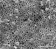 uniform and pinhole-free films that are highly conformal-that is, they exactly follow the contours of objects that are oddly shaped by the standards of other film deposition processes. uniform and pinhole-free films that are highly conformal-that is, they exactly follow the contours of objects that are oddly shaped by the standards of other film deposition processes.
Charles L. Dezelah, general manager at Picosun, ALD instrument manufacturer with headquarters in Espoo, Finland, and Detroit, says that ALD practitioners have historically thought of ALD as "just" a thin-film deposition technique. But he sees a much broader future for the method. 'With its unique layer-by-layer atomic precision, ALD is a virtually limitless tool for nanochemistry,' he says."
Source:
Click the link to read the full article:
Chemical & Engineering News: http://pubs.acs.org/cen/science/89/8931sci1.html
Image: Argonne National Laboratory
|
| |
|
Apple's Process for Fighting Finger Oils on Touch Surfaces
From PatentlyApple.com, August 12, 2011: "The third patent application of the day relates to applying an oleophobic coating to the surface of a material. In particular, this is directed to using a direct liquid application in a Physical Vapor Deposition ("PVD") chamber to apply the coating to the material. Apple states that as the user touches the surface of a device such as an iOS device, oils and other particles from the user's fingers could be deposited on the surface. This may adversely affect the appearance of the surface, especially if information is being displayed. One way to limit the amount of oils and particles deposited on the surface of portable devices is to apply an oleophobic treatment to the surface. However, this approach could be difficult to accomplish. Apple states that to prevent the deposition of oils on an electronic device surface, an oleophobic ingredient could be bonded to the electronic device surface. The oleophobic ingredient could be provided as part of a raw liquid material in one or more concentrations. To avoid adverse reactions due to exposure to air, heat, or humidity, the raw liquid material can be placed in a bottle purged with an inert gas during the manufacturing process." Source:
Click the link and scroll to the bottom of the web page to read the full article:
PatentlyApple.com: http://www.patentlyapple.com/patently-apple/2011/08/new-patents-surface-for-an-iphone-antenna-clip-solar-energy-and-a-new-oil-resistant-coating-for-ios-devices.html
|
| |
|
Designing Diamond Circuits for Extreme Environments
From Vanderbilt University, August 4, 2011, by David Salisbury: "There is a new way to design computer chips and electronic circuitry for extreme environments: make them out of diamond.
A team of electrical engineers at Vanderbilt University has developed all the basic components needed to create microelectronic devices out of thin films of nanodiamond. They have created diamond versions of transistors and, most recently, logical gates, which are a key element in computers.
"Diamond-based devices have the potential to operate at 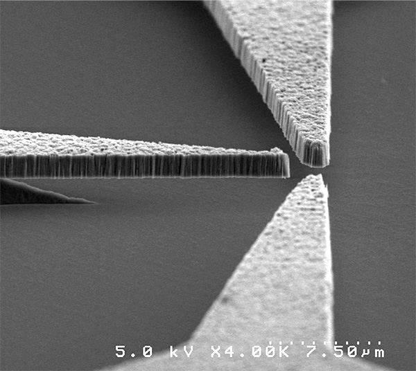 higher speeds and require less power than silicon-based devices," Research Professor of Electrical Engineering Jimmy Davidson said. "Diamond is the most inert material known, so our devices are largely immune to radiation damage and can operate at much higher temperatures than those made from silicon." higher speeds and require less power than silicon-based devices," Research Professor of Electrical Engineering Jimmy Davidson said. "Diamond is the most inert material known, so our devices are largely immune to radiation damage and can operate at much higher temperatures than those made from silicon."
The films are made from hydrogen and methane using a method called chemical vapor deposition that is widely used in the microelectronics industry for other purposes.
Potential applications include military electronics, circuitry that operates in space, ultra-high speed switches, ultra-low power applications and sensors that operate in high radiation environments, at extremely high temperatures up to 900 degrees Fahrenheit and extremely low temperatures down to minus 300 degrees Fahrenheit." Source: Click the link to read the full article: Vanderbilt University, Research News@Vanderbilt: http://news.vanderbilt.edu/2011/08/nanodiamond/ Image: Davidson Lab
|
| |
|
Graphene Creates Flexible Film to Rival ITO
From ElectroIQ.com, August 5, 2011, by Meredith Courtemanche: "Rice University's James Tour's Lab has created thin films from graphene that eliminate expensive, brittle indium tin oxide (ITO) films for touchscreen displays, solar panels, and LED lights. The see-through graphene-hybrid film is flexible, allowing integration into body-wearable electronics or building integrated photovoltaics (BIPV), among other commercial applications.
The Tour Lab's thin film combines a single-layer sheet of highly 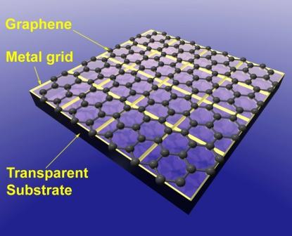 conductive graphene with a fine grid of metal nanowire. The combination outperformed ITO and competing materials at the Lab, offering better transparency and lower electrical resistance. The hybrid works better than pure graphene, which interacts too much with its substrate, Tour said. The fine metal mesh maintains conductivity without blocking transparency, added postdoctoral researcher Yu Zhu. The gaps in the nanowires make them unsuitable stand-alone components in conductive electrodes. The researchers settled on a grid of 5um aluminum nanowires." conductive graphene with a fine grid of metal nanowire. The combination outperformed ITO and competing materials at the Lab, offering better transparency and lower electrical resistance. The hybrid works better than pure graphene, which interacts too much with its substrate, Tour said. The fine metal mesh maintains conductivity without blocking transparency, added postdoctoral researcher Yu Zhu. The gaps in the nanowires make them unsuitable stand-alone components in conductive electrodes. The researchers settled on a grid of 5um aluminum nanowires."
Source: Click on the link to read the entire article:
ElectroIQ.com: http://www.electroiq.com/articles/stm/2011/08/graphene-creates-flexible-film-to-rival-ito.html
Image: Yu Zhu, Rice University
|
| | |
|
A New Approach to Scratch Resistance
From MIT News Office, August 17, 2011, by David L. Chandler: "A new way to analyze how coatings of tiny particles alter the properties of transparent plastic could help researchers create lightweight windows with nearly the strength of glass. The same method could also lead to high-strength, scratch-resistant coatings that could be applied to many different materials, according to the MIT researchers who developed the analysis.
The analysis used a polymer called poly(methyl methacrylate), or PMMA, which is widely used as a glass substitute. Known generically as acrylic, and sold under trademarks such as Lucite or Plexiglas, this material can be brittle and is far less resistant to scratching than glass.
Other researchers have added silica particles measuring just nanometers across to PMMA, creating a polymer-particle nanocomposite with much greater strength. But the MIT team, for the first time, has found a way to analyze the particle-polymer interactions of such coatings at the nanoscale, which could facilitate the discovery of improved coatings. Their work was reported in July in the journal Soft Matter."
Source: Click the link to read the full article.
MIT News: http://web.mit.edu/newsoffice/2011/scratch-resistance-0817.html
|
|
|
|
Smart Skin: Electronics that Stick and Stretch Like a Temporary Tattoo
From University of Illinois News Bureau, August 11, 2011, by Liz Ahlberg: "Engineers have developed a device platform that combines electronic components for sensing, medical diagnostics, communications and human-machine interfaces, all on an ultrathin skin-like patch that mounts directly onto the skin with the ease, flexibility and comfort of a temporary tattoo.
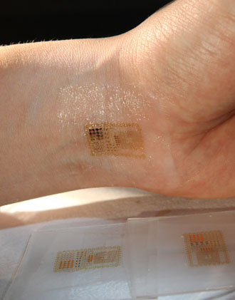 Led by John A. Rogers, the Lee J. Flory-Founder professor of engineering at the University of Illinois, the researchers described their novel skin-mounted electronics in the Aug. 12 issue of the journal Science. Led by John A. Rogers, the Lee J. Flory-Founder professor of engineering at the University of Illinois, the researchers described their novel skin-mounted electronics in the Aug. 12 issue of the journal Science.
The circuit bends, wrinkles and stretches with the mechanical properties of skin. The researchers demonstrated their concept through a diverse array of electronic components mounted on a thin, rubbery substrate, including sensors, LEDs, transistors, radio frequency capacitors, wireless antennas, and conductive coils and solar cells for power."
Source: Click the link to read the full article. University of Illinois, News Bureau: http://news.illinois.edu/news/11/0811skin_electronics_JohnRogers.html
Image: John Rogers
|
|
|
|
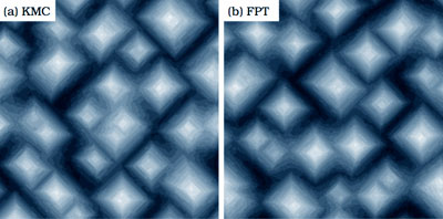
UT Physicist Accelerates Simulations of Thin Film Growth
From Ohio Supercomputer Center, May 17, 2011: "A Toledo, Ohio, physicist has implemented a new mathematical approach that accelerates some complex computer calculations used to simulate the formation of micro-thin materials.
Jacques Amar, Ph.D., professor of physics at the University of Toledo (UT), studies the modeling and growth of materials at the atomic level. He uses Ohio Supercomputer Center (OSC) resources and Kinetic Monte Carlo (KMC) methods to simulate the molecular beam epitaxy (MBE) process, where metals are heated until they transition into a gaseous state and then reform as thin films by condensing on a wafer in single-crystal thick layers. "One of the main advantages of MBE is the ability to control the deposition of thin films and atomic structures on the atomic scale in order to create nanostructures," explained Amar.
Amar settled on using a first-passage-time (FPT) approach to improve KMC processing speeds. FPT, sometimes also called first-hitting-time. Amar's FPT-KMC approach accelerated simulations by a factor of approximately 63 to 100 times faster than the corresponding KMC simulations for the fcc(100) model. The SOS model was improved by a factor of 36 to 76 times faster. For the Cu/Cu(100) tests, speed-up factors of 31 to 42 times faster were achieved for simulations using the full FPT distribution calculations."
Source: Click the link to read the full article.
Ohio Supercomputer Center: http://www.osc.edu/press/releases/2011/Amar11.shtml
Image: Ohio Supercomputer Center
|
|
|
|
Mitsubishi Electric Installs 6-Meter OLED Globe at Science Museum
From Mitsubishi Electric, June 1, 2011: Mitsubishi Electric Corporation announced today that it has installed a six-meter organic light-emitting display (OLED) globe at the National Museum of Emerging Science and Innovation in Tokyo, Japan. The OLED "Geo-Cosmos" display will be unveiled at the museum as the world's first large-scale spherical OLED screen.
Hanging 18 meters from the floor, the globe is an aluminum sphere covered with 10,362 OLED panels, each measuring 96 x 96 millimeters. Mitsubishi Electric used its scalable OLED technologies to create the globe, which replaces a globe comprising light emitting diodes (LEDs) to commemorate the museum's 10th anniversary. The globe will display scenes of clouds and other visions of the earth taken from a meteorological satellite. Projections will feature resolution of more than 10 million pixels, about 10 times greater than that of the LED display."

Source: Click the link to read the full article.
Mitsubishi Electronics: http://www.mitsubishielectric.com/news/2011/0601.html
Image: Mitsubishi Electronics
|
|
|
Do You Have an Interesting Article to Share?

Interested in sharing the latest news in vacuum coating technology? Forward us a link to an article you want to share with the rest of the SVC readership to publications@svc.org. Purchase advertising space in this newsletterby contacting SVC at svcinfo@svc.org.
Society of Vacuum Coaters
71 Pinon Hill Place NE
Albuquerque, New Mexico 87122
505-856-7188
|
| |
|
|
Vacuum Hardware and Chambers
Pfeiffer Vacuum offers a complete line of Trinos vacuum hardware as well as standard and custom chambers. Trinos offers the largest standard component selection with an extensive U.S. inventory. Learn More.
Pfeiffer Vacuum, Inc.
24 Trafalgar Square
Nashua, NH 03063-1988
Phone: 603-578-6500
Web site: www.trinos.com
E-Mail: trinos@pfeiffer-vacuum.com
|
| |
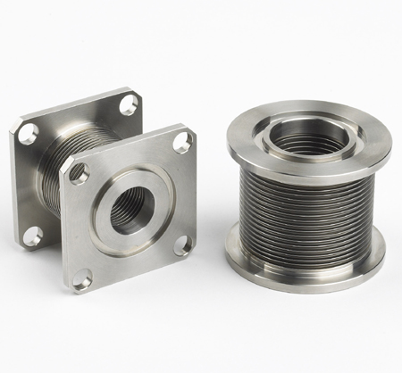
BellowsTech has launched a new web page focused entirely on the edge welded bellows technology process used to manufacture edge welded bellows, which offers a function unobtainable with any other metal bellows technologies known today. Learn More.
BellowsTech, LLC
Phone: 386-615-7530
www.bellowstech.com
Email: bellows@bellowstech.com
|
| |
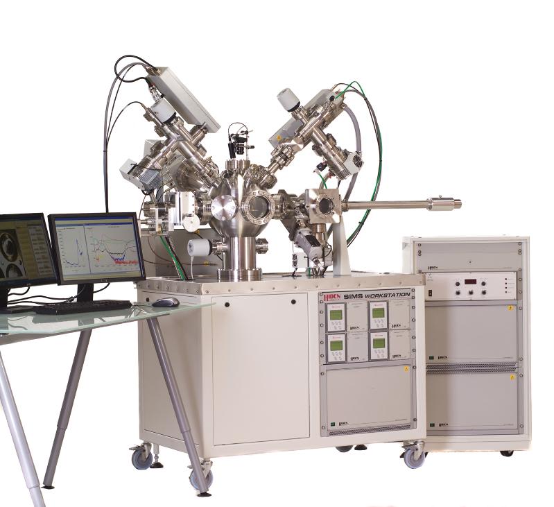
SIMS Workstation
A high performance SIMS instrument for:
- Thin film depth profiling
- Surface imaging
- Features new high sensitivity sputtered neutrals detection mode for quantitative analysis.
Learn more.
E-mail address: info@hiden.co.uk
Phone: +44 [0] 1925 445225 (UK)
or [1] 734 542 6666 (USA)
Website: www.HidenAnalytical.com
|
| |
VAT manufactures high quality vacuum valves for a variety of applications. Products include: gate, angle, fast-closing, transfer, pendulum, throttle, pressure control, all-metal and customized valves. Learn more.
Contact Us:
Phone: 781-935-1446
or 800-935-1446
E-Mail: US@vatvalve.com
|
| |
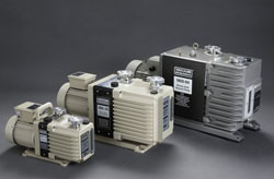
Dual Stage Rotary Vane Pumps
The VD Series dual stage, oil rotary vacuum pumps are available in pumping speeds from 600 - 800 l/min. They're lightweight and feature low noise with minimal vibration levels.
Learn More.
ULVAC Technologies, Inc.
Visit Us Online
Tel: 1-978-686-7550
E-mail: sales@us.ulvac.com
|
| |
INFICON thin film deposition controllers, monitors and accessories, including customizable sensors and feedthroughs, offer features, function and value targeted to your application. View our catalog and contact us today!
INFICON
www.inficon.com
E-mail: reachus@inficon.com
|
|
|
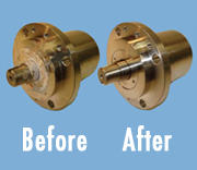
Rebuilt Feedthroughs
Rigaku rebuilds ferrofluid feedthroughs for all leading manufacturers and offers a warranty on rebuilt units. Most parts are stocked in inventory for fast turnaround. Learn More.
Rigaku Vacuum Products
www.rigakuvacuum.com
E-mail: vacuum-info@rigaku.com
Phone: 603-890-6001
|
| |
With Comdel's CB Series, Good Things Do Come in Small Packages
Comdel's CB Series brings the highest power and frequency while keeping its small package and lightweight design, and includes S-Technology for the ultimate process stability. Learn more.
Comdel
11 Kondelin Road
Gloucester, MA 01930
Tel: 978-282-0620 or 800-468-3144
Fax: 978-282-4980
www.comdel.com
info@comdel.com
|
| |
|
MDC's Bundled Engineered Solutions
MDC offers virtually every component required for vacuum coating applications. With MDC's standard chamber line you have the advantage of bundling these high quality pieces together without hours or weeks of special engineering. More...
MDC
engineered process solutions
www.mdcvacuum.com
|
| |
|
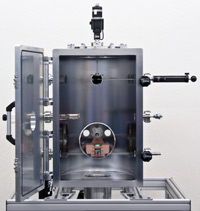
Choose Evatec's MSP sputter tool for high volume production in 3D technology and enjoy excellent thin film repeatabilities, a proven tool concept and a reliable partner.
Phone: (603) 669-9656
www.evatecnet.com
E-Mail:infoNA@evatecnet.com
|
| |
Bruker's New DektakXT™ Stylus Profiler
DektakXT™ sets a new standard in high-performance thin-film measurements with better than 5Å step height repeatability, scanning up to 40% faster, and a single-arch design, that improves the system's noise floor. Learn More. Bruker Corporation 520-741-1044 productinfo@bruker-nano.com |
| |
|
Rotary Vane Pumps
Stock to 4 Weeks
3 to 64 CFM, 6 to108 m3/hour. All voltages, 1 and 3 phase. Fomblin/Krytox available. 2 year parts and labor warranty, satisfaction guaranteed.
Vacuum Research Corporation Phone: 800/426-9340
Web: www.vacuumresearch.com
E-Mail: vrc@vacuumresearch.com
|
| |
|
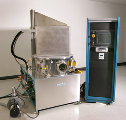
Dynavac's Diamond-Like Carbon Deposition System produces infrared and anti-reflection coatings for commercial and military applications on substrates up to 24" diameter.
www.dynavac.com
Telephone: 781-740-8600
E-Mail: sales@dynavac.com |
| |
|
Speed pump-down and vacuum performance with RediVac™ Vented Screws and Vacuum Baked O-Rings from
UC Components Inc.
www.uccomponents.com
|
| |
|

Evans Analytical Group (EAG) is the leading global provider of high quality surface analysis and materials characterization services to the films and coatings industry.
Evans Analytical Group
1.800.366.3867
|
| |
|
Veeco provides RF Linear Ion Sources for medium and large scale substrates featuring a broad power range and patented technology that provides reliability and performance.
To Learn More Visit:
www.veeco.com
970-221-1807
|
| |
|

Solid Sealing Technology designs and manufactures hermetic assemblies using metalizing, brazing and glass-ceramic sealing including standard and custom Feedthroughs/Connectors for extreme environments and UHV.
Contact:
Ph: 518-874-3600
Fax: 518-874-3610
info@solidsealing.com
|
| |
Nanovea manufactures Profilometers, Mechanical Testers & Tribometers to combine the most advanced testing capabilities in the industry. And unlike other manufacturers, Nanovea also provides Laboratory Services.
Learn More
www.nanovea.com
E-Mail: info@nanovea.com
Phone: 949-461-9292 |
| |
|
1st International Symposium on Transparent Conductive Coatings
October 4-6, 2011
Incheon, Korea
A Joint Symposium Sponsored by:
The Korean Institute of Surface Engineering (KISE)
-and-
Society of Vacuum Coaters
Now Accepting Papers on the Following Topics
- dry processes for transparent conductive coating
- wet processes for display devices
- materials and processes for energy conversion devices
- plasma generations and simulations
Learn More
Visit the KISE web site and click the TCC Symposium button.
|
| |
The 55th Annual SVC TechCon
April 28 - May 3, 2012
Santa Clara, California
|
| |
Now Available...
2012 Exhibit Prospectus

Exhibit Hours
Tues, May 1: 12-6 pm
Wed, May 2: 10 am-5 pm
-and-
2012 Call for Papers
 Abstract Submission Deadline Abstract Submission Deadline
October 14, 2011
Preview Both Today!
|
| |
SVC On-Location
Education Program
Bring High Quality, Practical Tutorials in PVD Processing and Vacuum Technology to Your Facility.
SVC Provides:
Recognized Instructors
Practical Information
A Schedule Convenient for You
Cost-Effective Training
Learn More...
|
| |
|