Welcome to the June issue of SVConnections. There still may be uncertainty in the grand scheme of the global economy, but science and technology continue to be the driving force behind its eventual recovery. This issue of SVConnections features the people and efforts behind the development of today's technology and the latest on technologies promising an exciting future.
You are welcome to share an interesting article on vacuum coating and related processes with the SVC community. E-mail us at publication@svc.org. |
| | |
|
Hydrogen Fuel Tech Gets Boost from Low-Cost, Efficienct Catalyst
From SLAC National Accelerator Laboratory, May 3, 2011:
"Scientists have engineered a cheap, abundant alternative to the expensive platinum catalyst and coupled it with a light-absorbing electrode to make hydrogen fuel from sunlight and water.
The discovery is an important development in the worldwide effort to mimic the way plants make fuel from sunlight, a key 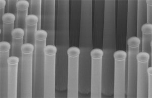 step in creating a green energy economy. It was reported last week in Nature Materials by theorist Jens Nørskov of the Department of Energy's SLAC National Accelerator Laboratory and Stanford University and a team of colleagues led by Ib Chorkendorff and Søren Dahl at the Technical University of Denmark (DTU). step in creating a green energy economy. It was reported last week in Nature Materials by theorist Jens Nørskov of the Department of Energy's SLAC National Accelerator Laboratory and Stanford University and a team of colleagues led by Ib Chorkendorff and Søren Dahl at the Technical University of Denmark (DTU). Hydrogen is an energy dense and clean fuel, which upon combustion releases only water. Today, most hydrogen is produced from natural gas which results in large CO2-emissions. An alternative, clean method is to make hydrogen fuel from sunlight and water. The process is called photo-electrochemical, or PEC, water splitting. When sun hits the PEC cell, the solar energy is absorbed and used for splitting water molecules into its components, hydrogen and oxygen. Progress has so far been limited in part by a lack of cheap catalysts that can speed up the generation of hydrogen and oxygen. A vital part of the American-Danish effort was combining theory and advanced computation with synthesis and testing to accelerate the process of identifying new catalysts. This is a new development in a field that has historically relied on trial and error. "If we can find new ways of rationally designing catalysts, we can speed up the development of new catalytic materials enormously," Nørskov said." Source: Click on the link to read the full article SLAC National Accelerator Laboratory: http://home.slac.stanford.edu/pressreleases/2011/20110502.htm Image: Christian D. Damsgaard, Thomas Pedersen and Ole Hansen, Technical University of Denmark |
|
|
|
New NanoMarkets Report Forecasts the Market for Energy Storage in the Solar Power Industry
From NanoMarkets.net, April 28, 2011: "Industry analyst firm NanoMarkets has just issued a new report that says the solar power industry will use $953 million (USD) in energy storage systems in 2016, rising to $1.5 billion in 2018. The report, Energy Storage Markets in the Solar Energy Industry is the latest in NanoMarkets' ongoing coverage of energy storage and renewable energy markets. A related report, Energy Storage Opportunities in the Wind Power Industry was issued in Q4 of 2010.
The demand for high energy density batteries is expected to surge to meet the needs of the growing number of utility-scale solar plants. Such plants are already being heavily promoted by large solar panel firms in anticipation of lowered PV subsidies for consumers. The growing trend towards grid-scale PV will also be fueled by anti-nuclear sentiments following the Japanese disasters. High energy density batteries for solar power storage are expected to reach revenues of $763 million by 2016.
In the wake of reduced feed-in tariffs for PV, large commercial users will want to better manage the energy they generate and sell back to utilities. NanoMarkets believes that energy storage will become a key part of this new management effort and his trend will help take sales of lead-acid and lead-carbon batteries for solar power storage to $465 million by 2016."
Source:
Click on the link to read the full article
NanoMarkets.net: Full article here
|
| |
|
How Intel's New Three-Dimensional Transistors Went from Lab to Fab
From MIT Technology Review, May 6, 2011, by Katherine Bourzac: "Intel's new three-dimensional transistor design announced early this week, is the culmination of more than a decade of research and development work that began in a lab at the University of California, Berkeley in 1999.
The 22-nanometer transistors, which Intel says will make chips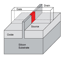 37 percent faster and half as power hungry, will be used for every element on the company's 22-nanometer scale chips, including both the logic and memory circuits. Processors that use the "tri-gate" transistors have been demonstrated in working systems, and the company will begin volume production in the second half of this year. It's unclear just how device-makers will take advantage of the chips, but they're likely to enable improved battery life and greater sophistication for portable devices, as well as faster processing for desktops and servers. 37 percent faster and half as power hungry, will be used for every element on the company's 22-nanometer scale chips, including both the logic and memory circuits. Processors that use the "tri-gate" transistors have been demonstrated in working systems, and the company will begin volume production in the second half of this year. It's unclear just how device-makers will take advantage of the chips, but they're likely to enable improved battery life and greater sophistication for portable devices, as well as faster processing for desktops and servers.
Intel turned to the new design because existing designs have begun running up against a performance roadblock. Conventional transistors are made up of a metal structure called a gate that's mounted on top of a flat channel of silicon. The gate controls the flow of current through the channel from a source electrode to a drain electrode. With every generation of chips, the channel has gotten smaller and smaller, enabling companies like Intel to make faster chips by packing in more transistors. But it has become more difficult for the gate to fully cut off the flow of current. Leaky transistors that don't turn off completely waste power."
Source:
Click on the link to read the entire article:
MIT Technology Review: http://www.technologyreview.com/computing/37536/?mod=chthumb
Image: Technology Review
|
|
|
|
OCI Bets on Polysilicon
From Chemical & Engineering News, April 29, 2011, by Jean-Francois Tremblay: "South Korea's OCI will spend nearly $1.7 billion to build what it claims will be the world's largest single polysilicon plant. The company expects the 24,000-metric-ton-per-year facility to come on-line in 2013.
Polysilicon is used to create semiconductor wafers as well as high-efficiency photovoltaic cells. Both markets are healthy, although the photovoltaic industry, OCI's target sector, is growing faster.
OCI acknowledges that it is investing at a time when the polysilicon market is becoming oversupplied. In South Korea and elsewhere, many producers are expanding capacity. "But by building larger, you get economies of scale," an OCI spokeswoman tells C&EN. The firm's polysilicon will be able to compete even if prices drop, she contends."

Source: Click on the link to read the full article
Chemical & Engineering News: http://pubs.acs.org/cen/news/89/i18/8918notw6.html
Image: IHS iSuppli
|
| |
|
Nanomaterials Underpin ITO Alternative Coming to Market
From +Plastic Electronics, May 3, 2011, by Sara Ver-Bruggen: "Recent months have seen unprecedented commercial progress by nanomaterial products developed as alternatives to transparent conductive oxide (TCO) materials such as indium tin oxide (ITO).
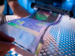 The deals and investments by developers, including California, US-headquartered Cambrios and Beneq in Finland, suggest that confidence in the performance of some nanomaterials-based TCO alternatives is becoming more assured within newer segments of the display and wider microelectronics industry. Cambrios recently revealed a leading smartphone incorporates its transparent conductor technology, which is based on silver nanowire solutions coated onto PET film. The ClearOhm product is used in the phone's touchscreen interface. Cambrios partnered with Synaptics, a provider of touchscreen modules and systems, to bring its technology to market. The collaboration marks the first commercial debut of transparent electrodes in the smartphone market that use alternative materials to TCOs such as ITO, which is less suited - due to its brittleness - to touchscreen electronics." Source: Click on the link to read the entire article: +Plastic Electronics: http://www.plusplasticelectronics.com/consumerelectronics/nanomaterials-underpin-ito-alternatives-coming-to-market-30344.aspx Image: +Plastic Electronics
|
| |
|
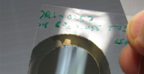
In Situ Surface-Roughness Measuring Topographer
From SPIE Newsroom, March 28, 2011, by Robert E. Parks: "Measuring surface roughness or finish is one of the more difficult measurements for large mirrors or lenses. In general, the measurand is too large to place on the stage of a surface-roughness measuring device, so that an indirect measurement must be made using replicas. In addition, the long mechanical path between interference objective and sample on traditional microscope-based profilers makes them prone to vibrations caused by environmental noise, which disturbs temporal phase-shifting measurements.
Our research team developed the MicroFinish Topographer  (MFT), and the entire unit is kinematically supported directly on the surface that needs to be measured using three nylon balls. The short, stiff mechanical-support loop between the three balls and the interference objective means that measurements can be made directly, without the need for replicas or vibration-isolation equipment. Any environmental noise couples in phase to both the device and the surface, so there is no net displacement between them, and phase-shifting measurements are unaffected. (MFT), and the entire unit is kinematically supported directly on the surface that needs to be measured using three nylon balls. The short, stiff mechanical-support loop between the three balls and the interference objective means that measurements can be made directly, without the need for replicas or vibration-isolation equipment. Any environmental noise couples in phase to both the device and the surface, so there is no net displacement between them, and phase-shifting measurements are unaffected.
The MFT consists of a point-source microscope that incorporates a Mirau interference objective, a piezoelectric transducer (PZT) to phase shift the objective, and 4Sight software to drive the PZT and analyze the interference pattern. The basic MFT is no different than other temporal phase-shifting roughness-measuring interferometers, except for its symmetric, short-coupled, stiff mechanical-support structure. This is in contrast to the vibration-prone stages of most other similar devices."
Source: Click the link to read the full article:
SPIE Newsroom: http://spie.org/x47484.xml?ArticleID=x47484
Image: John Davis, Steward Observatory Mirror Laboratory, University of Arizona
|
| |
Free Standing Single Walled Carbon Nanotube Thin Film
From Aalto University, May 13, 21011: "Single-walled CNTs (SWCNTs) are a unique family of materials exhibiting diverse useful chemical and physical properties.
Thin films of SWCNTs have many unique properties such as high porosity and specific surface area, low density, high ratio of optical transmittance to sheet resistance, high thermal conductivity and chemical sensitivity, and tunable metallic and semiconducting properties.
Recently researchers from Department of Applied Physics at Aalto University (Finland) in collaboration with Canatu Ltd. (Finland) have discovered a simple and rapid method to prepare thin multifunctional single-walled carbon nanotube films without any substrate (free-standing films). Usually SWCNT films are prepared from suspensions of SWCNTs by a liquid filtration. This method typically involves several time and resource consumingand potentially detrimental liquid dispersion and purification steps ending up with dense SWCNT networks on a filter, which have a transfer issue. Moreover, preparation of free-standing films bythe vacuum-filtration method is still a challenging task."
Source: Click the link to read the full article:
Aalto University: http://www.aalto.fi/en/current//news/view/2011-05-13/
Image: Aalto University
|
| |
|
Exploring the Superconducting Transition in Ultra Thin Films
From Brookhaven National Laboratory News, April 27, 2011: "Like atomic-level bricklayers, researchers from the U.S. Department of Energy's (DOE) Brookhaven National Laboratory are using a precise atom-by-atom layering technique to fabricate an ultrathin transistor-like field effect device to study the conditions that turn insulating materials into high-temperature superconductors. The technical break-through, which is described in the April 28, 2011, issue of Nature, is already leading to advances in understanding high-temperature superconductivity, and could also accelerate the development of resistance-free electronic devices.
"Understanding exactly what happens when a normally insulating copper-oxide material transitions from the insulating to the superconducting state is one of the great mysteries of modern physics," said Brookhaven physicist Ivan Bozovic, lead author on the study.
One way to explore the transition is to apply an external electric field to increase or decrease the level of "doping" - that is, the concentration of mobile electrons in the material - and see how this affects the ability of the material to carry current. But to do this in copper-oxide (cuprate) superconductors, one needs extremely thin films of perfectly uniform composition - and electric fields measuring more than 10 billion volts per meter. (For comparison, the electric field directly under a power transmission line is 10 thousand volts per meter.)
Bozovic's group has employed a technique called molecular beam epitaxy (MBE) to uniquely create such perfect superconducting thin films one atomic layer at a time, with precise control of each layer's thickness. Recently, they've shown that in such MBE-created films even a single cuprate layer can exhibit undiminished high-temperature superconductivity.*
Now, they've applied the same technique to build ultrathin superconducting field effect devices that allow them to achieve the charge separation, and thus electric field strength, for these critical studies.
Source: Click the link to read the full article:
Brookhaven National Laboratory News: http://www.bnl.gov/bnlweb/pubaf/pr/PR_display.asp?prID=1268
|
| |
|
Oak Ridge National Lab Develops 3-D Nanocone Solar Cell with High Efficiency Potential
From PV-Tech.org, May 3, 2011, by Syanne Olson: "Jun Xu and his team of researchers at the Oak Ridge National Laboratory have created a 3-D nanocone-based solar cell, which is said to enhance the light-to-power conversion efficiency by almost 80%. The solar cell is constructed using n-type nanocones made from zinc oxide, which perform as the junction framework and electron conductor , and are enveloped by a p-type semiconductor consisting of polycrystalline cadmium telluride, which act as the principal photon absorber channel and hole conductor.
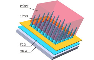 "To solve the entrapment problems that reduce solar cell efficiency, we created a nanocone-based solar cell, invented methods to synthesize these cells and demonstrated improved charge collection efficiency," said Xu, a member of ORNL's chemical sciences division. "To solve the entrapment problems that reduce solar cell efficiency, we created a nanocone-based solar cell, invented methods to synthesize these cells and demonstrated improved charge collection efficiency," said Xu, a member of ORNL's chemical sciences division.
Using this technology, Xu and his team are said to have reached a light-to-power conversion efficiency of 3.2%, compared to the 1.8% efficiency of the traditional planar structure from the same materials. The researchers point to the solar materials distinctive electric field distribution, which allows for an efficient charge transport, the combination of nanocones using economical proprietary methods and the reduction of defect and voids in semiconductors as important features of the technology that allow for the enhanced conversion rate. Interestingly, the team maintains that due to the efficient charge transport, the new solar cell is said to be able to endure defective materials and therefore lessen the cost of producing next-generation solar cells."
Source: Click on the link to read the entire article:
PV-Tech.org: full article
Image: PV-Tech.org
|
| | |
|
Solar Junction Breaks World Record with 43.5% Efficient CPV Production Cell
From Solar Junction, April 14, 2011: "Solar Junction, a developer of high efficiency multi-junction cells for the concentrated photovoltaic (CPV) market, today announced it
has set a world-record for 43.5 percent efficiency on a commercial-ready production cell. This achievement was, in part, supported under the U.S. Department of Energy
(DOE) PV Incubator Program, managed through DOE's National Renewable Energy Laboratory (NREL). The cell's efficiency was confirmed by NREL's Measurement and
Characterization Laboratory. The 5.5 mm x 5.5 mm production cell tops the current record by 1.2 percent and is significantly higher than the average efficiency gain achieved by previous record holders. The Solar Junction cell measured a peak
efficiency of 43.5 percent at greater than 400 suns and still maintained an efficiency as high as 43 percent out to 1,000 suns.
Solar Junction's cells incorporate the company's proprietary adjustable spectrum latticematched, A-SLAM™ technology, which enables the company to more optimally partition
the solar spectrum for maximum efficiency and greater reliability. Increases in CPV cell efficiencies are a key driver for improving CPV economics, with each cell efficiency gain
leveraged and multiplied in value by the components that account for the remaining 80 percent of total system costs."
Source: Click the link to read the full press release
Solar Junction: full press release
|
|
|
Do You Have an Interesting Article to Share?

Interested in sharing the latest news in vacuum coating technology? Forward us a link to an article you want to share with the rest of the SVC readership to publications@svc.org. Purchase advertising space in this newsletterby contacting SVC at svcinfo@svc.org.
Society of Vacuum Coaters
71 Pinon Hill Place NE
Albuquerque, New Mexico 87122
505-856-7188
|
| |
|
|
 
Veeco provides RF Linear Ion Sources for medium and large scale substrates featuring a broad power range and patented technology that provides reliability and performance.
To Learn More Visit:
www.veeco.com
970-221-1807
|
| |
|

Solid Sealing Technology designs and manufactures hermetic assemblies using metalizing, brazing and glass-ceramic sealing including standard and custom Feedthroughs/Connectors for extreme environments and UHV.
Contact:
Ph: 518-874-3600
Fax: 518-874-3610 info@solidsealing.com
|
| |

Nanovea manufactures Profilometers, Mechanical Testers & Tribometers to combine the most advanced testing capabilities in the industry. And unlike other manufacturers, Nanovea also provides Laboratory Services.
Learn More
www.nanovea.com
E-Mail: info@nanovea.com
Phone: 949-461-9292 |
| |
|

$4,995 Dry Turbopump Station
The Pfeiffer Vacuum HiCube™ Eco vacuum station includes turbo and dry diaphragm pumps. It delivers a pumping speed of 67 l/s
and an ultimate pressure of <10-8 mbar. Learn More.
Pfeiffer Vacuum, Inc.
24 Trafalgar Square
Nashua, NH 03063-1988
Phone: 603-578-6500
hicube@pfeiffer-vacuum.com
|
| |
BellowsTech manufactures edge welded metal bellows and assemblies for UHV chambers and semiconductor equipment with high cycle life, complete customization, and competitive pricing.
Learn More.
BellowsTech, LLC
Phone: 386-615-7530
www.bellowstech.com
Email: bellows@bellowstech.com
|
| |
EQP Mass and Energy Analyser for Plasma Diagnostics
- Plasma ion analyser for +ve and -ve ion analysis
- Neutrals and neutral radical detection
- For correlation of plasma parameters with film quality Learn More
E-mail address: info@hiden.co.uk Phone: +44 [0] 1925 445225 (UK) or [1] 734 542 6666 (USA) Website:www.HidenAnalytical.com
|
| |
VAT manufactures high quality vacuum valves for a variety of applications. Products include: gate, angle, fast-closing, transfer, pendulum, throttle, pressure control, all-metal and customized valves. Learn more.
Contact Us:
Phone: 781-935-1446
or 800-935-1446
E-Mail: US@vatvalve.com
|
| |
|
Gas Analysis - Low Cost RGA
ULVAC offers three compact quadrupole mass spectrometers - the low cost Qulee BGM, Qulee CGM for high pressures and Qulee HGM for the highest sensitivity. Learn More.
ULVAC Technologies, Inc.
Visit Us Online
Tel: 1-978-686-7550
E-mail: sales@us.ulvac.com
|
| |
INFICON thin film deposition controllers, monitors and accessories, including customizable sensors and feedthroughs, offer features, function and value targeted to your application. View our catalog and contact us today!
INFICON
www.inficon.com
E-mail: reachus@inficon.com
|
| |
Rebuilt Feedthroughs
Rigaku rebuilds ferrofluid feedthroughs for all leading manufacturers and offers a warranty on rebuilt units. Most parts are stocked in inventory for fast turnaround. Learn More.
Rigaku Vacuum Products
www.rigakuvacuum.com
E-mail: vacuum-info@rigaku.com
Phone: 603-890-6001
|
| |
Comdel's CV Series Delivers Stable Power for VHF Applications
Comdel's CV series offers stable power at frequencies from 30 to 80 MHz. Ideal for use in VHF plasma systems, solar/photovoltaics, CW and pulsed laser systems. Learn more.
Comdel
11 Kondelin Road
Gloucester, MA 01930
Tel: 978-282-0620 or 800-468-3144
Fax: 978-282-4980
www.comdel.com
info@comdel.com
|
| |
|
MDC's Bundled Engineered Solutions
MDC offers virtually every component required for vacuum coating applications. With MDC's standard chamber line you have the advantage of bundling these high quality pieces together without hours or weeks of special engineering. More...
MDC
engineered process solutions
www.mdcvacuum.com
|
| |
|

Choose Evatec's MSP sputter tool for high volume production in 3D technology and enjoy excellent thin film repeatabilities, a proven tool concept and a reliable partner. Contact Evatec's dedicated USA office for all your local sales and service requirements in thin film technology.
Phone: (603) 669-9656 www.evatecnet.com E-Mail: infoNA@evatecnet.com
|
| |
Bruker's New DektakXT™ Stylus Profiler
DektakXT™ sets a new standard in high-performance thin-film measurements with better than 5Å step height repeatability, scanning up to 40% faster, and a single-arch design, that improves the system's noise floor. Learn More. Bruker Corporation 520-741-1044 productinfo@bruker-nano.com |
| |
|
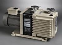
Rotary Vane Pumps
Stock to 4 Weeks
3 to 64 CFM, 6 to108 m3/hour. All voltages, 1 and 3 phase. Fomblin/Krytox available. 2 year parts and labor warranty, satisfaction guaranteed.
Vacuum Research Corporation Phone:800/426-9340
Web: www.vacuumresearch.com
E-Mail: vrc@vacuumresearch.com
|
| |
|
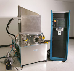
Dynavac's Diamond-Like Carbon Deposition System is a precise and reliable tool for commercial and military infrared applications. The system produces DLC films that create a hard, smooth, antireflective film across an array of optical surfaces, including germanium and silicon products. A 24" diameter cathode accommodates many substrate sizes.
www.dynavac.com
Telephone: 781-740-8600
E-Mail: sales@dynavac.com |
| |
|

Speed pump-down and vacuum performance with RediVac™ Vented Screws and Vacuum Baked O-Rings from
UC Components Inc.
www.uccomponents.com
|
| |
SVC On-Location
Education Program
Bring High Quality, Practical Tutorials in PVD Processing and Vacuum Technology to Your Facility.
SVC Provides:
Recognized Instructors
Practical Information
A Schedule Convenient for You
Cost-Effective Training
Learn More...
|
| |
Save the Dates!
The 55th Annual SVC TechCon
April 28 - May 3, 2012
Santa Clara, California
 Featuring Two Symposia Featuring Two Symposia
"Lab to Fab" Thin Film Manufacturing Processes
-and-
New Materials and Processes for Photovoltaics Manufacturing
Call for Papers Available
July 2011
|
| |
|