In just a few days, the Society of Vacuum Coaters will proudly host its 54th Annual TechCon in Chicago, IL. The TechCon embodies SVC's mission to promote technical excellence by providing a global forum to inform, educate, and engage the members, the technical community, and the public on all aspects of vacuum coating, surface engineering and related technologies.
SVConnections also serves as an extension of this mission, providing relevant information to our membership and beyond throughout the entire year. So take advantage of the valuable information found in the April issue and we hope to see you in person from April 16-21 to share, learn and network at the TechCon in Chicago. |
| | |
|
New Plastics Can Conduct Electricity
From The University of New South Wales (UNSW), Sydney, Australia; by Bob Beale, Feb 22, 2011
"A newly discovered technique makes it possible to create a whole new array of plastics with metallic or even superconducting properties.
Plastics usually conduct electricity so poorly that they are used to insulate electric cables bu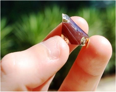 t, by placing a thin film of metal onto a plastic sheet and mixing it into the polymer surface with an ion beam, Australian researchers have shown that the method can be used to make cheap, strong, flexible and conductive plastic films. t, by placing a thin film of metal onto a plastic sheet and mixing it into the polymer surface with an ion beam, Australian researchers have shown that the method can be used to make cheap, strong, flexible and conductive plastic films.
The research has been published in the journal ChemPhysChem by a team led by Professor Paul Meredith and Associate Professor Ben Powell, both at the University of Queensland, and Associate Professor Adam Micolich of the UNSW School of Physics. This latest discovery reports experiments by former UQ Ph.D. student, Dr Andrew Stephenson.
Ion beam techniques are widely used in the microelectronics industry to tailor the conductivity of semiconductors such as silicon, but attempts to adapt this process to plastic films have been made since the 1980s with only limited success - until now."
Read the full article at on the UNSW web site: http://www.science.unsw.edu.au/news/new-plastics-can-conduct-electricity/
Source:
The University of New South Wales: http://www.science.unsw.edu.au/
Image: Adam Micolich
|
|
|
|
Iron Nitride Powder Produced as Substitute for Rare Metal
From Tech-On!, Tech and Industry Analysis from Asia, by Tsunenori Tomioka and Nikkei Monozukuri:
"A Japanese research group succeeded in producing powder of iron nitride (Fe16N2) by the gram. The group, which consists of Migaku Takahashi and Tomoyuki Ogawa, professor and associate professor, respectively, at a graduate school of Tohoku University, and researchers at Toda Kogyo Corp, succeeded in generating Fe16N2 powder with a purity of 91% and a reproducibility for the first time in the world.
The group has been researching on Fe16N2 as a candidate for a powerful magnet material that does not use any rare earth element in the "Rare Metal Substitute Materials Development Project" led by New Energy and Industrial Technology Development Organization (NEDO).
The produced Fe16N2 powder has a particle diameter of several tens to several hundreds of nanometers. Its saturation magnetization is 230emu/g at a temperature of 50K and 221emu/g at room temperature, which is higher than that of pure iron (1emu/g =4n x 10-7Wb·m/kg).
Though its magnetic crystalline anisotropy, which is proportionate to coercive field strength, is low, its maximum energy product, which determines the strength of magnet, is expected to be 100MGOe (796kJ/m3), which is more than 30% higher than that of sintered magnets using neodymium-iron-boron (Nd-Fe-B)."
Source: Clink on link to read full article.
Tech-On!: http://techon.nikkeibp.co.jp/english/NEWS_EN/20110307/190128/
|
| |
|
Market for Vacuum-Coated Products Still Growing
From Paper, Film and Foil Converter (PFFC), February 2011. pages 24-28, by Dr. William Llewellyn, AWA Alexander Watson Associates, Amsterdam, The Netherlands: 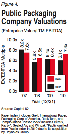
World demand for vacuum coated products continues to thrive, driven by demand in India and China and the expanding flexible display market. Currently, Asia Pacific holds 49% of the vacuum-coated films and papers market, followed by Europe (25%) and North America (18%). The report describes the regions and their markets, such as Polypropylene,, PET, and metalized paper. South America is a new entry and is advancing quickly in vacuum-coated materials production.
Source:
Click on the link to read the entire article:
Paper, Film and Foil Converter: http://pffc-online.com/flexpack/still-growing-coat-lam-0201/#
Image: Capital IQ |
|
|
|
New Government Report Identifies Supply Risks for Thin-Film PV Materials
From Solar Industry, February 2011, by Jessica Lillian:
U.S. Department of Energy (DOE) completed a 'Critical Materials Strategy' report for the clean energy technologies including PV. Gallium, indium and tellurium supply risks were analyzed.
Gallium supply can be increased faster than tellurium or indium. Most gallium worldwide is produced as a byproduct of treating bauxite and from zinc-processing residues. The long-term supply is reported to be very stable and very strong.
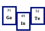 Indium is extracted as a by-product of zinc processing. PV manufacturers must compete with industries, such as flat-panel display industry, which are expected to experience major growth before settling down in the next 1 to 2 years. Indium was determined to have a short-term supply risk. China is reported to have 50% of world's indium supply. Since 2005, Canada, Australia and other countries are developing more indium production capacity. Indium is extracted as a by-product of zinc processing. PV manufacturers must compete with industries, such as flat-panel display industry, which are expected to experience major growth before settling down in the next 1 to 2 years. Indium was determined to have a short-term supply risk. China is reported to have 50% of world's indium supply. Since 2005, Canada, Australia and other countries are developing more indium production capacity.
Tellurium's supply story is different because the majority goes to thin-film PV industry for CdTe module fabrication. First Solar is the major CdTe module manufacturer currently. Paul Markowitz, senior analyst at market research firm NanoMarkets "does not expect another manufacturer to approach First Solar's output for at least another four or five years." Tellurium's short-term supply will have stresses placed by the solar market, while the long-term availability looks good.
Critical material strategies of other nations are included in the report.
Source:
Solar Industry, February 2011, pp. 28-30: http://issuu.com/zackinpublications/docs/sim1102_online?mode=a_p
Read the full DOE Critical Materials Strategy report: http://www.energy.gov/news/documents/criticalmaterialsstrategy.pdf
Image: Star Science
|
| |
|
Voiding Defects: New Technique for More Efficient LEDs
From North Carolina State University, January 25, 2011, by Matt Shipman: "Light-emitting diodes (LEDs) are an increasingly popular technology for use in energy-efficient lighting. Researchers from North Carolina State University have now developed a new technique that reduces defects in the gallium nitride (GaN) films used to create LEDs, making them more efficient.
LED lighting relies on GaN thin films to create the diode structure that produces light. The new technique reduces the number of defects in those films by two to three orders of magnitude. "This improves the quality of the material that emits light," says Dr. Salah Bedair, a professor of electrical and computer engineering at NC State and co-author, with NC State materials science professor Nadia El-Masry, of a paper describing the research. "So, for a given input of electrical power, the output of light can be increased by a factor of two - which is very big." This is particularly true for low electrical power input and for LEDs emitting in the ultraviolet range.
 The researchers started with a GaN film that was two microns, or two millionths of a meter, thick and embedded half of that thickness with large voids - empty spaces that were one to two microns long and 0.25 microns in diameter. The researchers found that defects in the film were drawn to the voids and became trapped - leaving the portions of the film above the voids with far fewer defects. The researchers started with a GaN film that was two microns, or two millionths of a meter, thick and embedded half of that thickness with large voids - empty spaces that were one to two microns long and 0.25 microns in diameter. The researchers found that defects in the film were drawn to the voids and became trapped - leaving the portions of the film above the voids with far fewer defects.
Source: Click on the link to read the entire article:
North Carolina State University Newsroom: http://news.ncsu.edu/releases/wmsbedairganvoids/
Image: Lukasz Tylec
|
| |
|
High-Sensitivity, Broad-Range Vacuum Gauge Using Nanotubes for Micromachined Cavities
From NASA TechBriefs, NASA Jet Propulsion Laboratory, January 2011: "A broad-range vacuum gauge has been created by suspending a single-walled carbon nanotube (SWNT) (metallic or semiconducting) in a Schottky diode format or in a bridge conductor format, between two electrically charged mesas. SWNTs are highly sensitive to molecular collisions because of their extremely small diameters in the range of 1 to 3 nanometers. The measurement parameter will be the change in conductivity of SWNT due to decreasing rate of molecular collisions as the pressure inside a chamber decreases."
Source: Click the link to read the full article:
NASA TechBriefs: http://www.techbriefs.com/component/content/article/9023
|
| |
Nanopatterned Metallic Films Make Wavelength-Tunable Lenses
From SPIE Newsroom, January 7, 2011, by Danhong Huang, et al.: "There is considerable current interest in shaping the spatial dependence of the intensity of light transmitted through a metal film pierced by a 1D array of slits with subwavelength widths. Particular attention has been paid to the use of such structures as metallic nanoscale lenses. In contrast to conventional dielectric refractive lenses, whose focusing ability degrades as their dimensions decrease to the operational wavelength level, nanoscale slit lenses retain their focusing ability in this limit. Because of their planar geometries, they are simpler to fabricate at these dimensions than dielectric lenses, and use of metal rather than a dielectric provides a higher index contrast that leads to a stronger focusing capability. Finally, they focus light in the far rather than the near field, unlike, e.g., perfect (negative-index metamaterial) lenses.
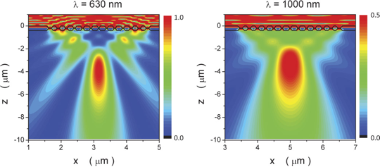
However, it is not necessary to have slits that completely pierce the metallic film to achieve such focusing. A suitable modulation of the film thickness can produce the same effect. We have demonstrated this by calculating numerically the spatial distribution of the intensity of light transmitted through a metal film with surfaces modeled by two aligned, reversed arrays of nanogrooves of finite depth, sandwiched between vacuum and a dielectric substrate."
Source: Click the link to read the full paper:
SPIE.org: http://spie.org/x43641.xml?ArticleID=x43641
Image: Danhong Huang and SPIE.org
|
| |
|
Toward Third-Generation Solar Cells
From SPIE Newsroom, January 7, 2011, by Zetian Mi,
et al.: "Recently, indium nitride (InN) nanowires have emerged as a promising candidate for a range of nanoscale electronic, photonic, and biochemical devices. Extensive studies have shown that they exhibit a small direct energy bandgap (∼0.6-0.7eV), high electron mobility, and small electron effective mass. However, application devices require precise control of the charge properties of InN nanostructures. The currently reported InN nanowires and films are generally n-type degenerate with a residual doping of ∼1×1018cm−3 or higher. 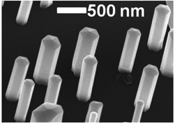 The uncontrollable electron density has made it extremely difficult to achieve p-type doping and to accurately determine many fundamental properties of InN, thereby severely limiting practical device applications. We have succeeded in growing, for the first time, nearly intrinsic (that is, undoped, or extremely pure) InN. In addition, we have experimentally demonstrated InN nanowire solar cells, opening up exciting possibilities for indium gallium nitride (InGaN) nanowire-based, full-solar-spectrum, third-generation solar cells. The uncontrollable electron density has made it extremely difficult to achieve p-type doping and to accurately determine many fundamental properties of InN, thereby severely limiting practical device applications. We have succeeded in growing, for the first time, nearly intrinsic (that is, undoped, or extremely pure) InN. In addition, we have experimentally demonstrated InN nanowire solar cells, opening up exciting possibilities for indium gallium nitride (InGaN) nanowire-based, full-solar-spectrum, third-generation solar cells.
Conventional InN nanowires grown on silicon (Si) generally exhibit a tapered morphology, with the presence of large densities of dislocations and stacking faults due to the uncontrolled wire nucleation associated with spontaneous growth, as well as the formation of an amorphous silicon nitride (SiNx) layer at the InN/Si heterointerface. In our approach, we first deposited a thin (∼0.5nm) In layer on the substrate surface before introducing any nitrogen species, which forms nanoscale In liquid droplets at elevated temperatures and can promote the nucleation and growth of vertically aligned InN nanowires. The wires are remarkably straight, with identical top and bottom sizes, compared to any previously reported InN nanowires. Detailed transmission electron microscopy studies further confirm that the wires are nearly free of dislocations and stacking faults.
Source: Click the link to read the full paper:
SPIE.org: http://spie.org/x43643.xml?highlight=x2400&ArticleID=x43643
Image: Zetian Mi and SPIE
|
| |
|
Memory Training for Metal Structures
From Leibniz Institute for New Materials (INM), saarbruken, Germany, January 26, 2011: "Designing metal structures with a memory is the work of the Leibniz Institute for New Materials junior research group "Metallic Microstructures". Researchers, led by Dr. Andreas Schneider, are investigating how to train structured surfaces to switch their special properties on and off.
"This can be achieved with a suitable combination of heat treatment and deformation." Then the material memorizes the shape at a higher and lower temperature. This two-way memory effect allows for making the surface structures switchable via temperature. Thus, for example, friction and adhesion on surfaces can be specifically switched on and off."
"The group's second focus of research is based on 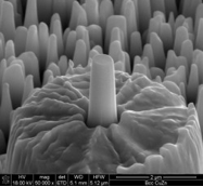 microstructures that influence the strength of a metal surface. "We recognize that a metal is the stronger the smaller the structures on the surface are made. Many thin pillars bear a temple roof better than a few thick pillars", explains the junior researcher. The research group studies which influences lead to this effect." microstructures that influence the strength of a metal surface. "We recognize that a metal is the stronger the smaller the structures on the surface are made. Many thin pillars bear a temple roof better than a few thick pillars", explains the junior researcher. The research group studies which influences lead to this effect."
"The scientists produce the microstructures among other things with a scanning ion microscope, removing minutest amounts of metal in layers from the surface. At the end, micropillars with a fixed diameter and a fixed height protrude from the metal. With a stamp, which presses from above onto the pillars, the scientists test the forces which the pillars withstand, before they cave in."
Source: Click on the link to read the entire article:
Leibniz Institute for New Materials (INM): http://www.inm-gmbh.de/2011/01/memory-training-for-metalstructures/
Image: Leibniz Institute for New Materials (INM)
|
| | |
|
Molecules in Thin Films Remain Frozen at a Temperature in Molten Material
From AZO Nanotechnology, March 31, 2011, by Cameron Chai: "A team of researchers at the U.S. Department of Energy's Brookhaven National Laboratory have found that thin molecular films continue to be in a frozen state at a temperature where the bulk material is in the molten state.
These molecules in thin films are deployed in several applications like organic solar cells and biosensors and perceiving the basic features of these molecular films could bring about enhanced devices.
The research was published in Physical Review Letters' April edition and the researchers directly perceived 'surface freezing' phenomenon at the hidden layer between solid surfaces and heavy liquids.
Ben Ocko, Physicist at Brookhaven, worked with researchers from France-based European Synchrotron Radiation Facility (ESRF) and Israel-based Bar-Ilan University. He has stated that the surface of most of the materials will begin to disarray and ultimately melt at a particular temperature where the bulk material remains to be in a solid state. Because outer molecules are less constricted than those molecules that are filled in the inner layers and they can easily travel around. He added that in surface freezing, the interface layers freeze before the bulk material."
Source:
AZO Nanotechnology: www.azonano.com: http://www.azonano.com/news.asp?newsID=22090
|
|
|
|
Japan Quake: Tracking the Status of Electronics Fabs in the Wake of Disaster
From EETimes.com: The EE times has put together the most up-to-date information available about the status of chip fabs 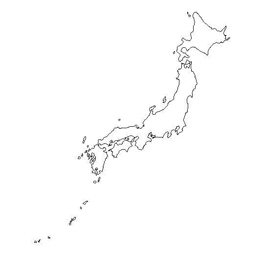 and other facilities that have been impacted by damage to structures, equipment and infrastructure stemming from the March 11 earthquake and tsunami in Japan. Listed are chip makers, alphabetically by company, with pages detailing the status of equipment and materials suppliers, consumer electronics companies and automakers, and test and measurement companies. Japan supplies about 60% of the world's electronic grade silicon. Japan is the fifth electronic supplier in the world with 63.3 $B in annual chip revenue according to IHS-ISuppli. and other facilities that have been impacted by damage to structures, equipment and infrastructure stemming from the March 11 earthquake and tsunami in Japan. Listed are chip makers, alphabetically by company, with pages detailing the status of equipment and materials suppliers, consumer electronics companies and automakers, and test and measurement companies. Japan supplies about 60% of the world's electronic grade silicon. Japan is the fifth electronic supplier in the world with 63.3 $B in annual chip revenue according to IHS-ISuppli.
Read the latest updates at:
EETimes.com: http://www.eetimes.com/electronics-news/4214018/Japan-quake--Tracking-the-status-of-fabs-in-wake-of-disaster
|
|
|
Do You Have an Interesting Article to Share?

Interested in sharing the latest news in vacuum coating technology? Forward us a link to an article you want to share with the rest of the SVC readership to publications@svc.org. Purchase advertising space in this newsletterby contacting SVC at svcinfo@svc.org.
Society of Vacuum Coaters
71 Pinon Hill Place NE
Albuquerque, New Mexico 87122
505-856-7188
|
| |
|
|
Visit Dynavac at the
SVC TechCon - Booth 1116
Dynavac's Odyssey 450 Deposition System is a small-scale tool providing an affordable, turnkey solution for uniform deposition of many materials. Its flexible architecture supports multiple upgrades and processes, including sputtering, evaporation, and ion assist. With its compact footprint, it is ideal for process development, pilot production, and research laboratories in both industry and universities.
www.dynavac.com
Telephone: 781-740-8600
E-Mail: sales@dynavac.com |
| |
|
Visit Veeco at the
SVC TechCon - Booth 1105

Veeco provides RF Linear Ion Sources for medium and large scale substrates featuring a broad power range and patented technology that provides reliability and performance.
To Learn More Visit:
www.veeco.com
970-221-1807
|
| |
|
Visit Solid Sealing Technology at the SVC TechCon
Booth 1033

Solid Sealing Technology designs and manufactures hermetic assemblies using metalizing, brazing and glass-ceramic sealing including standard and custom Feedthroughs/Connectors for extreme environments and UHV.
Contact:
Ph: 518-874-3600
Fax: 518-874-3610 info@solidsealing.com
|
| |
|
Visit Nanovea at the
SVC TechCon - Booth 1034

Nanovea manufactures Profilometers, Mechanical Testers & Tribometers to combine the most advanced testing capabilities in the industry. And unlike other manufacturers, Nanovea also provides Laboratory Services.
Learn More
www.nanovea.com
E-Mail: info@nanovea.com
Phone: 949-461-9292 |
| |
|
Visit Pfeiffer Vacuum at the SVC TechCon - Booth 1020

Vacuum Hardware and Chambers
Pfeiffer Vacuum offers a complete line of Trinos vacuum hardware as well as standard and custom chambers. Trinos offers the largest standard component selection with an extensive U.S. inventory. Learn More.
Pfeiffer Vacuum, Inc.
24 Trafalgar Square
Nashua, NH 03063-1988
Phone: 603-578-6500
Web site: www.trinos.com
E-Mail: trinos@pfeiffer-vacuum.com
|
| |
Visit BellowsTech LLC at the
SVC TechCon - Booth 1235

BellowsTech metal bellows withstand high high vacuum applications with low leak rates to ensure a hermetic seal, and are leak tight to 1x10⁻⁹ cc/He. Learn More.
BellowsTech, LLC
Phone: 386-615-7530
Fax: 386-615-7973
Email: bellows@bellowstech.com
|
| |
The Hiden HPR-30 is a residual gas analyser configured for analysis of gases and vapours in vacuum processes and for vacuum diagnostics.
Learn more.
E-mail address: info@hiden.co.uk
Phone: +44 [0] 1925 445225 (UK)
or [1] 734 542 6666 (USA)
Website: www.HidenAnalytical.com
|
| |
Visit VAT Inc. at the
SVC TechCon - Booth 1226
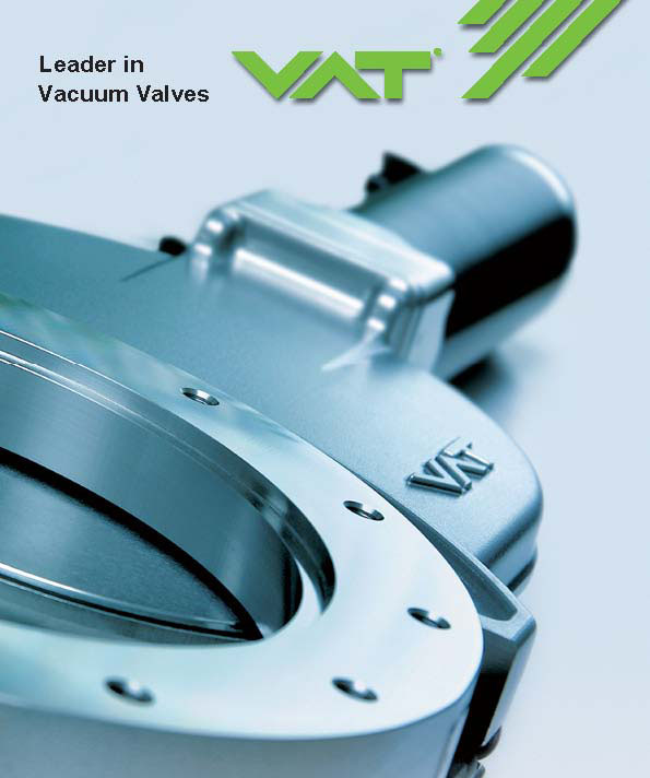
VAT manufactures high quality vacuum valves for a variety of applications. Products include: gate, angle, fast-closing, transfer, pendulum, throttle, pressure control, all-metal and customized valves. Learn more.
Contact Us:
Phone: 781-935-1446
or 800-935-1446
E-Mail: US@vatvalve.com
|
| |
Visit Ulvac Technologies at the SVC TechCon - Booth 1023
 Roll Coating System Roll Coating System ULVAC's SPW-030 roll coating system is capable of processing 300 mm wide substrate compositions including thin-gauge metal rolls and polymeric materials for R&D and Pilot-scale production. Learn More
ULVAC Technologies, Inc.
Visit Us Online
Tel: 1-978-686-7550
E-mail: sales@us.ulvac.com
|
| |
Visit INFICON at the
SVC TechCon - Booth 206

INFICON thin film deposition controllers, monitors and accessories, including customizable sensors and feedthroughs, offer features, function and value targeted to your application. View our catalog and contact us today!
INFICON
www.inficon.com
E-mail: reachus@inficon.com
|
| |
Visit Rigaku Vacuum Products at the SVC TechCon
Booth 1102

Custom Feedthrough Assemblies
Rigaku offers custom-engineered solutions from simple feedthroughs to feedback controlled subsystems for managing motion. This includes function-enhanced products and clean/vacuum magnetic rotary seals for robots. Learn More
Rigaku Vacuum Products
www.rigakuvacuum.com
E-mail: vacuum-info@rigaku.com
Phone: 603-890-6001
|
| |
Comdel Delivers Two
Power Supplies in One
Comdel's CDX provides two power supplies in one. Our compact design reduces space, electrical and plumbing, and spare inventory requirements.
Learn more.
Comdel
11 Kondelin Road
Gloucester, MA 01930
Tel: 978-282-0620 or 800-468-3144
Fax: 978-282-4980
www.comdel.com
info@comdel.com
|
| |
|
Visit MDC Vacuum Products at the SVC TechCon - Booth 1112
MDC's Bundled Engineered Solutions
MDC offers virtually every component required for vacuum coating applications. With MDC's standard chamber line you have the advantage of bundling these high quality pieces together without hours or weeks of special engineering. More...
MDC
engineered process solutions
www.mdcvacuum.com
|
| |
|
Visit Evatec at the
SVC TechCon - Booth 101

Choose Evatec's MSP sputter tool for high volume production in 3D technology and enjoy excellent thin film repeatabilities, a proven tool concept and a reliable partner. Contact Evatec's dedicated USA office for all your local sales and service requirements in thin film technology.
Phone: (603) 669-9656
www.evatecnet.com
E-Mail: infoNA@evatecnet.com
|
| |
|
Visit Bruker Corporation at the
SVC TechCon - Booth 409

Bruker's new DektakXT™ Stylus Profiler Features better than 5Å repeatability, enabling critical nanometer-level surface measurements for the microelectronics, semiconductor, solar, HB-LED and materials science industries. Learn More. Bruker Corporation 520-741-1044 productinfo@bruker-nano.com |
| |
|
Visit Vacuum Research Corporation at the
SVC TechCon - Booth 521

Rectangular Port Vacuum Valves
Ports to 220 X 1400 mm; 8 X 55 inch. Aluminum, Steel, or Stainless Steel. (RoHS) 2002/95/EC Compliant. Auto Close or Open on Power Fail. NW and ISO Gauge & Roughing Ports. Vacuum Research Corporation Phone:800/426-9340
Web: www.vacuumresearch.com
E-Mail: vrc@vacuumresearch.com |
| |
|
SVC TechCon Lake Cruise Networking Event

Tuesday Evening, April 19
7:00 p.m. - 9:30 p.m.
Cost per Person: $89.00
Includes buffet dinner, live entertainment and transportation between the Hyatt Regency Chicago on the Riverwalk and Navy Pier.
Purchase your tickets for this unique networking event while registering for the TechCon or at the TechCon before noon Monday, April 18.
|
| |
|