|
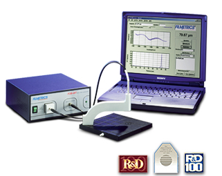
Filmetrics Thin-Film Thickness Measurement Systems
-Measure thickness from 1nm to 1mm
-Measure refractive index and other properties
-Used in thousands of applications worldwide
We offer the industry's only complete line of thin-film
measurement instruments. With our 24-hour online
"Hands On" support, expert help is only a minute away.
Contact:
www.filmetrics.com
858-573-9300 |
|
The R.D.
Mathis Company
specializes in the fabrication of high vacuum evaporation sources for thin film
coating industries. We offer a comprehensive selection of tungsten, molybdenum
and tantalum sources through our catalog and offer custom fabrication to meet
your specific coating needs. Our "LV Series" Low Voltage, High
Current Power Supplies and "GP 100" Inert Gas Purifier compliment
your evaporation process. Contact: www.rdmathis.com 562-426-7049
|
|
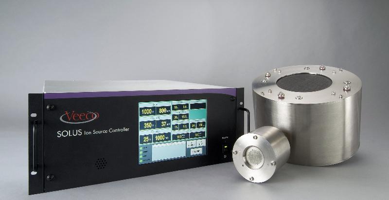
Veeco's
new SOLUS™ DC Ion Source Controller features a state-of-the-art precision control system
design providing reliable and stable power for ion source operation in all
types of processes. Integrated
power modules and gas flow control with ratio capabilities allow for optimal
ion source control and performance in the most demanding process environments. To Learn More Visit: www.veeco.com/SOLUS 970-221-1807
| 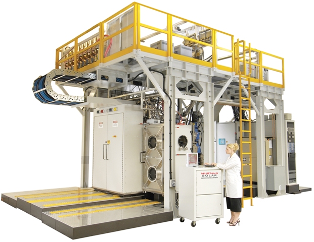
Mustang Vacuum Systems Orion Roll to Roll Deposition Systems
Substrate: Up to 10,000 FT
length, 1000 MM wide flexible substrates configured with 1-10 deposition
sources for precision and speed.
Deposition zones are individually configurable for PVD sputter,
evaporation, co-evaporation and sublimation enabling the next generation of
thin film technologies.
Visit Us
Email: inquiries@mustangvac.com
|
|

Solid Sealing Technology specializes in the design and manufacture of highly engineered hermetic products using metalizing, brazing, glass-ceramic sealing, welding, and critical assembly. SST manufactures industry standard and custom designed Vacuum Feedthroughs, Coaxial Connectors, Multi-Pin Connectors, Thermocouples, and Isolators for high temperature, UHV, and high pressure applications.
Contact:
Ph: 518-874-3600
Fax: 518-874-3610
info@solidsealing.com
| 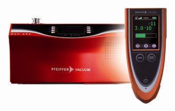
Helium Leak Detector with Wireless Remote
SmartTest(TM) portable helium leak
detector is rugged, easy to use and now comes with wireless remote so you can
operate at distances up to 300'. It comes with a user selected backing pump to
match any application and with vacuum and sniffer standard operating modes.
SmartTest provides the smallest detectable leak rate for helium: 5 x 10-12
mbar l/s.
Learn more.
|
ULVAC
offers three compact quadrupole mass spectrometers - the low cost Qulee
BGM, Qulee CGM for high pressures and Qulee HGM for the highest
sensitivity. All feature ease-of-operation and an integrated display and
control eliminates the need for a PC. One-touch control displays the
partial pressure in Torr, mbar, or Pascal
of He, H2O, N2, O2, O2/N2
ratio and user selected gas. Learn More
Contact:
978-686-7550
sales@us.ulvac.com
|
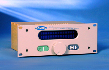
Power Your Electrostatic
Chucks with Comdel
With more than 30 models
from 1 to 10 kV, Comdel has the ESC power supply that's right for your
application, with bipolar or unipolar options, low stored energy and continuous
current limit for protection from surges/arcs and built in RF filters for
device protection and unsurpassed clamping. Variable control and fully programmable with analog, RS232 or
DeviceNet interface. Learn more.
Comdel11 Kondelin
Road
Gloucester, MA
01930
Tel: 978-282-0620 or
800-468-3144
Fax: 978-282-4980 www.comdel.com info@comdel.com |
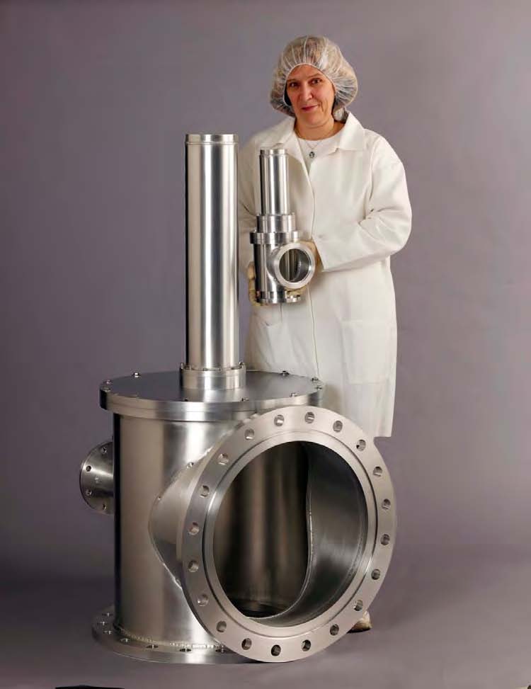
Steel and Aluminum High Vacuum Poppet Valves
Aluminum, Stainless or Mild Steel Valves with flanges to match
diffusion & Cryo pumps. Electroless nickel optional on steel valves. High
conductance full opening port. Leak tested to better than 5 X 10⁻¹⁰ scc/sec.
RoHS compliant and CE marked. Phone: 800-426-9340 Web: www.vacuumresearch.com Email: vrc@vacuumresearch.com |
|
MEWASA has expanded the manufacturing possibilities of its
bellows production, allowing the manufacture of bellows up to 1100mm in diameter.
Combined with the modern PC-based control, our machine provides the flexibility
to weld arbitrary bellows profiles, including oval shaped bellows with inside
dimensions of 66.7 to 117.5mm. MEWASA
has widened its capabilities, offering greater design solutions to meet your engineering
applications, whether it is larger dimensions or different profile shapes.
Contact: Ira Miller, General Manager,
Mewasa North America
i.miller@mewasa.ch Tel: 520-797-6980
|
800.245.1656 salesus@lesker.com www.lesker.com
Global manufacturer &
distributor of vacuum products. With our three divisions-The Vacuum Mart™,
Process Equipment Division, & Materials Division-we are your One Supplier
for a Complete Vacuum Solution. Offering quality products and quick delivery
from our worldwide warehouses. Exclusive distributor for Solvay Solexis'
Fomblin® and Galden® products for vacuum pumps & heat
transfer applications.
|
Make your life easier with
Evatec's advanced "Thin Film
Toolbox" Seamless
integration of film design software, a proprietary strategy generator for layer
termination, process recipe generation,download of process and finally coating itself enable manufacture of the
highest quality optical coatings time after time.
For information contact your local office.
Phone: +1 603
669-9656 . www.evatecnet.com
Mail: infoNA@evatecnet.com |

Speed
pump-down and vacuum performance with RediVac™ Vented Screws and Vacuum Baked
O-Rings from
UC
Components Inc. www.uccomponents.com | 
International Conference on HIPIMS
Sheffield Hallam University
Sheffield, United Kingdom
July 5-7, 2010
Featuring Two SVC Tutorial Courses
Click the links for course description, topical outline and detailed syllabus
Thin Film Growth and Microstructure Evolution
(Joseph Greene)
Sputter Deposition in Manufacturing
(David Glocker)
Click here for More Details
|

Innovation by Surface Technology
View this short and colorful video, displaying how vacuum coating plays a role in friction reduction and wear protection surfaces, micro and sensor technology, applications of optical coatings, photocatalysis, and transparent scratch protection.
Watch it Now!
|
|
|
|
|
Countless modern conveniences have traveled the journey from infancy to maturity; but few of us can claim to have been in close touch with the science, technology and vision behind their development. SVConnections is designed to illuminate the work and progress of those individuals and organizations whose breakthroughs and discoveries have led to yet another amazing process or gadget, enriching our lives. Read this latest snapshot of today's developments and stay on top of their impact on our personal and business lives.
|
Thin Film
Photovoltaic Manufacturing Equipment: Proprietary
or off-the-shelf?
It appears that equipment manufacturers targeting thin film
photovoltaic manufacturing are coming up against serious barriers to
entry. Some firms making cells and solar panels appear to prefer to
design and build their own fabrication equipment. According to NanoMarkets, the
TFPV industry will have a capacity of around 29 GWp and will be spending about
$4 billion on manufacturing equipment by 2015.
More at Thin Film Today:
|
|
Global PVD Industry Expected to be Worth Almost $15
Billion by 2014
From www.azom.com, May
6, 2010
According
to a new technical market research report, PHYSICAL VAPOR DEPOSITION (PVD):
GLOBAL MARKETS (MFG015D) from BCC Research, the value of the global PVD
industry was nearly $9 billion 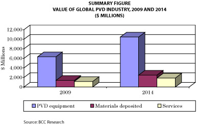 in 2009, but is expected to increase to more
than $14.8 billion in 2014, for a 5-year compound annual growth rate (CAGR) of
10.7%. The
largest segment of the market, PVD equipment, is projected to increase at a
CAGR of 10.5% to nearly $10.5 billion in 2014, after being valued at nearly
$6.4 billion in 2009.
Materials
deposited, which make up the second-largest segment of the market, are
estimated at $1.4 billion in 2009, and are expected to increase at a 5-year
CAGR of 12.2% to reach more than $2.5 billion in 2014.
The
services segment is projected to have a CAGR of 9.8%, with values of nearly
$1.2 billion in 2009 and nearly $1.9 billion in 2014.
The
PVD industry has expanded over the past several decades. More sophisticated
manufacturing and fabrication techniques and smaller-sized products have
broadened the demand for vapor-deposited materials. New and existing products
require materials that can be delivered by vacuum deposition of films on a
growing variety of substrates. (Click the image to
read the full article on www.azom.com)
Image: www.azom.com
|
|
Graphene
for All-Plastic Electronics: New
light-emitting electrochemical cell contains no metal electrode
By Belle Dume, Optics.org, April 27, 2010
Organic
light-emitting diodes (OLEDs) are increasingly being used in everyday
applications like televisions, camera displays and mobile phones. However,
despite using carbon-based materials as the light-emitting layer, previous
devices needed at least one metal electrode. Now, researchers in Sweden and the
US have used graphene as the transparent cathode in a device similar to an
OLED, called a light-emitting electrochemical cell (LEC). The device is one of
the first truly organic, or "plastic" electronic devices.
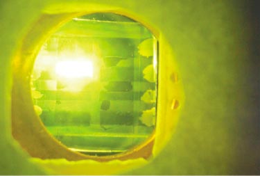 OLEDs
contain an electroluminescent layer that is made of an organic semiconductor
material sandwiched between two electrodes, at least one of which is
transparent. OLEDs are not only more environmentally friendly and easy to
process than conventional light sources, they can also generate photons across
a range of colours to produce white light. Devices made from OLEDs run on
little electricity too. OLEDs
contain an electroluminescent layer that is made of an organic semiconductor
material sandwiched between two electrodes, at least one of which is
transparent. OLEDs are not only more environmentally friendly and easy to
process than conventional light sources, they can also generate photons across
a range of colours to produce white light. Devices made from OLEDs run on
little electricity too.
Manish
Chhowalla's group at Rutgers University in the US began with graphite and
oxidized flakes of graphene oxide from the graphite in an acidic solution.
After filtering the suspension and transferring the resulting material to a
quartz substrate, the film was then reduced and annealed at high temperatures
in an oven containing argon/helium.
(click the image for the full article on http://optics.org)
Image: ACS Nano |
NIST-the
TIP Manufacturing Competition
The U.S. Department of Commerce has
announced a new manufacturing competition offering funding for approximately 25
projects totaling $25 million. The competition offers cost-shared funding for
innovative research on manufacturing and biomanufacturing on materials, advances
and critical processes. The due date for proposals is June, 15 2010. The 2010 TIP competition is open to research proposals in three areas: 1) Process
scale-up, integration and design for materials advances-addresses how new
materials move from the laboratory to full production. 2) Predictive
modeling for materials advances and materials processing-using the power of
modern analysis, modeling and computation to streamline the design and
production scale-up of new materials by more accurately predicting their
performance. 3) Critical
process advances-novel production technologies that dramatically improve the
processing of new materials or resolve important bottlenecks and inefficiencies
in the production of existing materials. Click here to link to the program at NIST Review the proposal link |
Magnetic
Thin Films and Nanostructures: Patterning
New Properties
By Professor Robert Stamps, University
of Western Australia, from AZoNano.com, May 18, 2010
Exceptional
advances in the control of material properties has been achieved, through
careful manipulation of geometry on nano- and sub-nanometre length scales, in
magnetoelectronics and nanomagnetism. Advanced techniques now allow for the
creation of structures patterned on sub-micron length scales in three
dimensions. New phenomena has been discovered in patterned magnets that can be
strongly controlled by ion bombardment, multilayering, and lithographic
patterning.
Examples
include: materials for microwave signal processing  technologies, whose
properties that can be tuned by magnetic and electric fields; high speed
switching of magnetization in elements used for data storage and spin
electronics; and manipulation of magnetic domains and domain walls in carefully
crafted structures that serve as model experimental systems for studies of
complex dynamics. technologies, whose
properties that can be tuned by magnetic and electric fields; high speed
switching of magnetization in elements used for data storage and spin
electronics; and manipulation of magnetic domains and domain walls in carefully
crafted structures that serve as model experimental systems for studies of
complex dynamics.
(click the image for the full article on www.azonano.com)
Image: azonano.com
|
New
Method Developed to Capture Fingerprints on Difficult Surfaces
By Gant Team, www.gantdaily.com, May
17,
2010
CSI
notwithstanding, forensics experts cannot always retrieve  fingerprints from
objects, but a conformal coating process developed by Penn State professors can
reveal hard-to-develop fingerprints on nonporous surfaces without altering the
chemistry of the print. fingerprints from
objects, but a conformal coating process developed by Penn State professors can
reveal hard-to-develop fingerprints on nonporous surfaces without altering the
chemistry of the print.
"As
prints dry or age, the common techniques used to develop latent fingerprints,
such as dusting or cyanoacrylate - SuperGlue - fuming often fail," said Robert
Shaler, professor of biochemistry and molecular biology and director of Penn
State's forensic sciences program.
This
happens because most of the techniques currently used for developing
fingerprints rely on the chemistry of the print. Fingerprints are made up of a
mixture of secretions from the body that reacts with different chemicals to
form a visible or fluorescent product. Infrared and x-ray imaging also target
specific chemicals left behind by the ridges and valleys in the skin.
"Lots
and lots of processes take advantage of the chemistry of fingerprints," said
Shaler. "This approach looks at the geometry of the fingerprints."
The
conformal coating applications suggested by Shaler and Ahklesh Lakhtakia,
Charles Godfrey Binder professor in engineering science and mechanics, use the
physical properties of the fingerprint, not the chemistry of the substances
left behind. In fact, the researchers believe that even after the fingerprints
are developed using the coating, forensics experts could sample the fingerprint
material to determine specifics about the person who left the prints.
(click the image to read the full article on www.gantdaily.com)
|
How Thin Films Melt
By J.R. Minkel, Physical World Focus, May 21, 2010
If
you heat a crystal that is just a few molecules thick, it melts differently
from a macroscopically thick crystal. A team using gel-like beads in liquid as
stand-ins for molecules examined melting in this "thin film" regime
by tracking the motion of each particle. As they report in the 21 May Physical
Review Letters, films thicker than four layers melt by passing through a phase
that is part liquid and part solid, whereas films of two to four layers melt
all at once. Single-layer films pass through a completely different phase
between solid and liquid, they found.
 Researchers
would like to know how phase transitions, such as from solid to liquid, change
when the substance is confined to fewer dimensions than the usual three. They
have fairly good theories on the melting of a single layer of molecules, but
more recently they have pursued the thin film regime--a few molecular layers.
Thin films have properties in common with both 2D and 3D, and their melting is
not well understood. For experiments, it's difficult to track individual
molecules, so researchers often turn to microscopic plastic spheres floating in
liquid, which act somewhat like molecules and can be tracked individually with
a microscope and video processing software. Researchers
would like to know how phase transitions, such as from solid to liquid, change
when the substance is confined to fewer dimensions than the usual three. They
have fairly good theories on the melting of a single layer of molecules, but
more recently they have pursued the thin film regime--a few molecular layers.
Thin films have properties in common with both 2D and 3D, and their melting is
not well understood. For experiments, it's difficult to track individual
molecules, so researchers often turn to microscopic plastic spheres floating in
liquid, which act somewhat like molecules and can be tracked individually with
a microscope and video processing software.
(click the image to read the full article on www.focus.aps.org)
Image: Y. Han, Hong Kong University of Science and Technology |
BP Solar Closes Last U.S. Plant Module
Manufacturing Line: moves to
China and India

BP
Solar has closed their Frederick, MD facility for making modules. As result
they will lay off 320 of 430 employees. Manufacturing of ingots and wafers will
continue at the plant. Even though the solar market has been growing rapidly,
cost cutting manufacturing has caused module production to go to China and
India because of lower labor costs. BP has joint projects with Xinjiang Sun
Oasis in Xi'an, China and Tata in India to produce modules. Unfortunately this
move is counter-productive for the creation of more clean technology
manufacturing in the U.S., as part of the U.S. Recovery Act.
Read the C&EN article
Original 2009 announcement by BP Solar
Image: BP Solar
|
New NIST Detector Counts Photons with 99% Efficiency
Scientists
at the National Institute of Standards and Techn ology (NIST) have developed the
world's most efficient single photon detector. The detector is able to count
individual particles of light traveling through fiber optic cables with roughly
99% efficiency. The efforts of Sae Woo Nam's NIST team could bring improvements
to secure electronic communication, advanced quantum computation and the
measurement of optical power. More information is at: http://www.nist.gov/eeel/optoelectronics/detector_041310.cfm ology (NIST) have developed the
world's most efficient single photon detector. The detector is able to count
individual particles of light traveling through fiber optic cables with roughly
99% efficiency. The efforts of Sae Woo Nam's NIST team could bring improvements
to secure electronic communication, advanced quantum computation and the
measurement of optical power. More information is at: http://www.nist.gov/eeel/optoelectronics/detector_041310.cfm
Image: NIST |
UCLA
Researchers Use New Microscope to "See" Atoms for First Time
Featured
In: Instrumentation, By EurekAlert, May 4, 2010
UCLA
researchers report in the April 30 edition of the journal Cell that they have
imaged a virus structure at a resolution high enough to effectively
"see" atoms, the first published instance of imaging biological
complexes at such a resolution.
The
research team, led by Hong Zhou, UCLA professor of microbiology, immunology and
molecular genetics, used cryo-electron microscopy to image the structure at 3.3
angstroms. An angstrom is the smallest recognized division of a chemical
element and is about the distance between the two hydrogen atoms in a water
molecule.
The
study, the researchers say, demonstrates the great potential of cryo-electron
microscopy, or Cryo-EM, for producing extremely high-resolution images of
biological samples in their native environment.
"This
is the first study to determine an atomic resolution structure through Cryo-EM alone,"
said Xing Zhang, a postdoctoral candidate in Zhou's group and lead author of
the Cell paper. "By proving the effectiveness of this microscopy
technique, we have opened the door to a wide variety of biological
studies."
With
traditional light microscopy, a magnified image of a sample is viewed through a
lens. Some samples, however, are too small to diffract visible light (in the
500 to 800 nm range, or 5,000 to 8,000 angstroms) and therefore cannot be seen.
To image objects at the sub-500 nm scale, scientists must turn to other tools,
such as atomic force microscopes, which use an atomically thin tip to generate
an image by probing a surface, in much the same way a blind person reads by
touching Braille lettering.
(Click here to learn more at www.biosciencetechnology.com)
|
Advanced
Production Technique Holds Promise for Silicon Rivals: Could silicon's choke
hold on the semiconductor universe be threatened?
By Levi
Beckerson (Blog) - May 25, 2010
Silicon
isn't the best semiconductor in the world. But among the features
keeping it
nearly ubiquitous in electronic devices is the 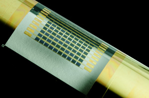 relative ease of
construction of
silicon-based chips in comparison to superior materials. As with just
about any
mass-produced product in the world, quality has long since taken the
back seat
to quantity. relative ease of
construction of
silicon-based chips in comparison to superior materials. As with just
about any
mass-produced product in the world, quality has long since taken the
back seat
to quantity.
One
contender for semiconductor superiority is gallium arsenide.
Unfortunately, as
one might be led to believe, the vapor deposition method typically
utilized to
create gallium arsenide is more costly than its silicon counterpart.
Fortunately for gallium arsenide, a group of DoE and NSF-funded
professors,
students and scientists based at the University of Illinois, has
pioneered a
new manufacturing process that will help even the field.
As
the previously utilized methods of gallium arsenide semiconductor
production
involved deposition to create a thin film, devices either needed to be
created
directly on the substrate or in a more typical wafer design which could
then be
clipped out into multiple pieces much like a standard silicon wafer
technique
used for manufacturing computer processor cores. The cleverness of the
UI
team's take on the thin films isn't in a revolutionary deposition
process, but
in using the same process over and over on the same substrate. By
utilizing the
same substrate multiple times, stacking the thin films on top of each
other,
they save time, money and manpower involved in producing the same amount
of
film in single sheets.
Click
image to read the full article on www.dailytech.com)
Image: John
Rogers, University of Illinois |
UC
Researcher to Contribute to the Next Generation of Space Vehicle
Voxy
News Engine, May 25, 2010
A
University of Canterbury engineer is working with American scientists on the
next generation of space vehicle.
Associate
Professor Susan Krumdieck, of UC's Department of Mechanical Engineering, has
been named as an investigator to work on the next generation of hypersonic
vehicle. The hypersonic vehicle, which will use scramjet engines and travel at
Mach 10-15, is regarded as a much more efficient replacement for the space
shuttle as it will be able to essentially fly to space.
The
project is being carried out by the US National Hypersonic Science Center for
Materials and Structures (NHSC) and is funded by the US Air Force and NASA. An
industrial contractor, Teledyne Scientific, and seven US universities are
involved in various aspects of research including materials, materials
processing, mechanics, atomistics and structures. Professor Krumdieck will be
working directly with David Marshall of Teledyne and Professor Rishi Raj of
University of Colorado at Boulder.
"It
is exciting to be working on the really challenging science problems
again," said Professor Krumdieck. "I don't know how many years in the
future this vehicle might be, or what the probability is that they will ever
figure out how to really do it, but that doesn't stop the Americans from trying
virtually impossible things. That is how they keep challenging their
researchers, and why they really do lead the world in science and advanced materials
engineering."
(Click here to read the full article on www.voxy.co.nz) |
|
A Message from the SVC President and Program Chairs
Click the image to read a special message from SVC President, Frank Zimone, and from the Program Chairs of the 2010 SVC TechCon in Orlando, FL.
|
Interested in Sharing the Latest News in Vacuum Coating Technology?

Interested in sharing the latest
news in vacuum coating technology? Forward us a link to an article you
want to share with the rest of the SVC readership to publications@svc.org. Purchase advertising space on this
newsletter by contacting SVC at svcinfo@svc.org.
|
|
Society of Vacuum Coaters 71 Pinon Hill Place, NE
Albuquerque, NM 87122
(505) 856-7188 Fax (505) 856-6716
www.svc.org E-mail: svcinfo@svc.org
|
|
|