Comdel
Delivers Low Frequency in a Small Lightweight Package Comdel's new CLB power supplies are available in
power ranges from 2500 to 12,000 Watts with standard fixed frequencies from 20
kHz to 2 MHz. The solid-state design is based on Comdel's proven RF amplifier
technology and provides precise and repeatable power control, ultra-stable
output and low cost of ownership.
Learn
more.
Comdel11 Kondelin Road
Gloucester, MA 01930
Tel: 978-282-0620 or 800-468-3144
Fax: 978-282-4980 www.comdel.com
info@comdel.com |
|
MEWASA
OFFERS r & d BELLOWS Test equipment capabilities Axial Endurance BELLOWS
testing BELLOWS UP TO OUTSIDE
Ø 500mm
CAN BE TESTED DYNAMICALLY Testing up to
100,000 cycles
possible Test Conditions: Inside: Vacuum Outside: Atmospheric Pressure
MEWASA Guarantees Highest Quality Swiss
Manufacturing of Edge
Welded Metal Bellows for Every Application Contact: i.miller@mewasa.ch or
520-797-6980 |
|

Filmetrics Thin-Film Thickness Measurement Systems
-Measure thickness from 1nm to 1mm
-Measure refractive index and other properties
-Used in thousands of applications worldwide
We offer the industry's only complete line of thin-film
measurement instruments. With our 24-hour online
"Hands On" support, expert help is only a minute away.
Contact:
www.filmetrics.com
858-573-9300 |
|
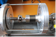
The R.D.
Mathis Company
specializes in the fabrication of high vacuum evaporation sources for thin film
coating industries. We offer a comprehensive selection of tungsten, molybdenum
and tantalum sources through our catalog and offer custom fabrication to meet
your specific coating needs. Our "LV Series" Low Voltage, High
Current Power Supplies and "GP 100" Inert Gas Purifier compliment
your evaporation process. Contact: www.rdmathis.com 562-426-7049
|
|
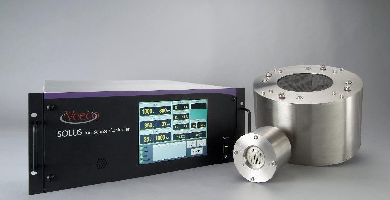
Veeco's
new SOLUS™ DC Ion Source Controller features a state-of-the-art precision control system
design providing reliable and stable power for ion source operation in all
types of processes. Integrated
power modules and gas flow control with ratio capabilities allow for optimal
ion source control and performance in the most demanding process environments. To Learn More Visit: www.veeco.com/SOLUS 970-221-1807
|
|

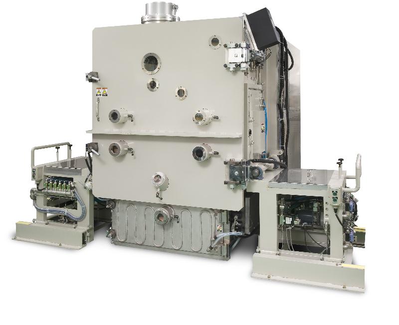
Mustang
Vacuum Systems - Colt 48 small batch and fast cycle sputtering system Provides plasma pre-treatment, metal
deposition and in chamber top coat in single vacuum process, resulting in
coatings with 92+% reflectivity. Fast
cycles ranging from 90 seconds to 3:30 minutes with exceptional uniformity of
+/-2% over 48"
Email:
inquiries@mustangvac.com
|
|

Solid Sealing Technology specializes in the design and manufacture of highly engineered hermetic products using metalizing, brazing, glass-ceramic sealing, welding, and critical assembly. SST manufactures industry standard and custom designed Vacuum Feedthroughs, Coaxial Connectors, Multi-Pin Connectors, Thermocouples, and Isolators for high temperature, UHV, and high pressure applications.
Contact:
Ph: 518-874-3600
Fax: 518-874-3610
info@solidsealing.com
|
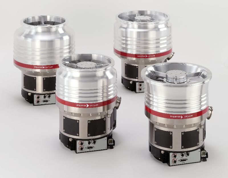
Turbopumps for High
Performance and Reliability
Pfeiffer
Vacuum HiPace turbopumps are available in pumping speeds from 10 to 3000
l/s. They feature an advanced rotor design providing high gas throughput
and exceptional compression for light gases. Innovative materials doubles rotor
life, while a proven bearing design ensures reliability, even in the harshest
coating applications. They offer a superior level of safety, including IP54 and
SEMI S2 protection classes. Contact
800-248-8254 or hipace@pfeiffer-vacuum.com
Pfeiffer Vacuum, Inc
www.pfeiffer-vacuum.com
Phone:
603-578-6500
|
Roll-Coating System
ULVAC's SPW-030
roll-coating system, designed for R&D and Pilot-scale production, is
capable of processing a 300 mm-wide web of various substrate compositions
including thin-gauge metal rolls and a variety of polymeric materials. The coating
system can be equipped with up to four (4) sputtering cathodes and an electron
beam evaporation source for depositing materials of varying compositions.
For further
information:
ULVAC Technologies, Inc.
Tel: 978-686-7550
Email: sales@us.ulvac.com
Web: www.ulvac.com
|
Home
of the Balzers BAK, Evatec delivers
thin film batch and cluster tools using evaporation, sputter, PECVD,
Microwave and ICP etch . Solutions for precision optics,
optoelectronics and semiconductor . Contact your local sales and service support
in North America for new sales, retrofits and upgrades. Telephone: 603.669.9656
|
800.245.1656 salesus@lesker.com www.lesker.com
Visit Kurt J. Lesker Company in Booth 303 at the SVC TechCon in
Orlando. We will be showcasing our wide breath of products for all your vacuum
needs. Offering thousands of production targets
and materials for immediate delivery.
Play our Details Matter game for a chance to win REI Camping Gear.
|

Speed
pump-down and vacuum performance with RediVac™ Vented Screws and Vacuum Baked
O-Rings from
UC
Components Inc. www.uccomponents.com |
|
SVC 2010 TechCon in Orlando, FL
Register for the TechCon NowPlease support SVC and book your hotel reservations at the Orlando World Center Marriott after you have completed the on-line registration for the TechCon. |
Visit our 2010 TechCon Sponsors!
|
|
|
|
|
Our technology is everywhere; impacting our lives with its innovative products and modern conveniences, and affecting our collective livelihood with its role in the global economy. SVConnections offers a taste of what's new in vacuum coating and related technologies and sheds light on how advances in science relates to our lives at home, at work and on the economic front. The Society of Vacuum Coaters' commitment to inform and educate our members, the technical community and the public on all aspects of vacuum coating, surface engineering and related processes drives this monthly e-publication. How will our technology affect your everyday life? Read on....
|
|
ECN Heads
Consortium to Develop a-Si Plastic Thin Films: Targets 7.5% Module Efficiencies
Posted February 22, 2010 on PV-tech.org  A program that started at
the beginning of the year and headed by Energy Research Centre of the
Netherlands (ECN), hopes to develop a new amorphous and microcrystalline
silicon thin film cell using plastics as the substrate foil. The three-year
'Silicon-Light' programme is subsidized by the European Commission in the
framework of the thematic research programme Energy in FP7. The R&D
consortium includes EPFL, University of Copenhagen, University of Valencia,
JiaoTong University of Shanghai, Umicore and VHF Technologies (Flexcell), the
hopeful commercial end-user of the programme. Flexcell is a subsidiary of
Q-Cells. A program that started at
the beginning of the year and headed by Energy Research Centre of the
Netherlands (ECN), hopes to develop a new amorphous and microcrystalline
silicon thin film cell using plastics as the substrate foil. The three-year
'Silicon-Light' programme is subsidized by the European Commission in the
framework of the thematic research programme Energy in FP7. The R&D
consortium includes EPFL, University of Copenhagen, University of Valencia,
JiaoTong University of Shanghai, Umicore and VHF Technologies (Flexcell), the
hopeful commercial end-user of the programme. Flexcell is a subsidiary of
Q-Cells.
To be able to use low-cost materials such as plastics, the Silicon-Light'
programme will develop low process temperatures (typically below 200ºC), using
plasma enhanced chemical vapour deposition (PECVD) processes.
(click on image to read the full article on www.pv-tech.org) Image: pv-tech.org
|
Photovoltaic
Breakthroughs Brighten Outlook for Cheap Solar Power: Novel materials might
make harvesting sunlight for electricity affordable
By David Biello, Scientific American, February 16, 2010
Enough sunlight bathes Earth's daytime half in an hour to
meet all human energy needs for a year. Sadly, there are several
problems with meeting human energy demands by tapping such abundant, free solar power-not least of which is the cost of
making semiconducting material that can cheaply harvest the power in sunlight.
But material improvements from the California Institute of Technology and IBM
might just lower the cost of solar power.
Graduate student Michael Kelzenberg and other materials scientists at Caltech
employed vertical crystals of silicon-microwires, like "blades of
grass," Kelzenberg says-to capture as much as 85 percent of the full
spectrum of incoming sunlight, the researchers report
in the February 14 Nature Materials.
(Scientific American is part of
Nature Publishing Group.) Their efficiency is almost as good as that of
traditional silicon wafers, yet they require just one percent of the silicon in
such wafers.
"With one one-hundredth of the material, we've gotten it to absorb 96
percent of the peak visible light," Kelzenberg says. "There's lots of
reasons to believe this could be scaled to make thin-film solar cells."
(click here to read the full article on www.scientificamerican.com) |
Gecko's
Lessons Transfer Well: Dry Printing of Nanotube Patterns to Any Surface Could
Revolutionize Microelectronics
From ScienceDaily - January 31, 2010
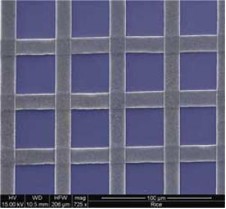 Watch a gecko walk up a wall. It defies gravity as it sticks
to the surface no matter how smooth it appears to be.
What's
happening isn't magic. The gecko stays put because of the electrical attraction
-- the van der Waals force -- between millions of microscopic hairs on its feet
and the surface.
The principle
applies to new research at Rice University reported this week in the online
version of the journal ACS Nano. But in this case, the hairs figuratively come
off the gecko and plant themselves on the wall.
Rice graduate
student Cary Pint has come up with a way to transfer forests of strongly
aligned, single-walled carbon nanotubes (SWNTs) from one surface to another --
any surface -- in a matter of minutes. The template used to grow the nanotubes,
with its catalyst particles still intact, can be used repeatedly to grow more
nanotubes, almost like inking a rubber stamp.
Pint is
primary author of the research paper, which also details a way to quickly and
easily determine the range of diameters in a batch of nanotubes grown through
chemical vapor deposition (CVD). Common spectroscopic techniques are poor at
seeing tubes bigger than two nanometers in diameter -- or most of the nanotubes
in the CVD "supergrowth" process.
(click the
image for full article on www.sciencedaily.com) Image: Rice University
|
Super-Thin Films
that Harvest Energy from Motion
Posted February 24, 2010 on www.azonano.com
Scientists are reporting an
advance toward scavenging energy from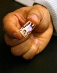 walking, breathing, and other natural
body movements to power electronic devices like cell phones and heart
pacemakers. walking, breathing, and other natural
body movements to power electronic devices like cell phones and heart
pacemakers.
In
a study in ACS' monthly journal, Nano Letters, they
describe development of flexible, biocompatible rubber films for use in
implantable or wearable energy harvesting systems. The material could be used,
for instance, to harvest energy from the motion of the lungs during breathing
and use it to run pacemakers without the need for batteries that must be
surgically replaced every few years.
Michael McAlpine and colleagues point out
that popular hand-held consumer electronic devices are using smaller and
smaller amounts of electricity. That opens the possibility of supplementing
battery power with electricity harvested from body movements. So-called
"piezoelectric" materials are the obvious candidates, since they
generate electricity when flexed or subjected to pressure. However,
manufacturing piezoelectric materials requires temperatures of more than 1,000
degrees F., making it difficult to combine them with rubber.
|
|
Crystal
Growth Points to Defect-Free Thin Films
Alexander E. Braun, Senior Editor -- Semiconductor
International, 2/1/2010
Cornell University (Ithaca, N.Y.) scientists are studying the
challenges that arise from the fact that to make semiconductor thin films,
layers of atoms must be grown in neat, crystalline sheets. While some materials
usually grow smooth crystals, others develop bumps and defects, leading
researchers to seek insights into how atoms arrange themselves into thin films.
Physics Pro fessor Itai Cohen, who leads the research,
indicated that the effort resulted from his colloidal suspension work.
"Colloids are a good model system for investigating atomic-scale
phenomena," he said. "The particles are small enough to behave like
atoms but still large enough to be observed under a microscope and manipulated
with optical tweezers. They're ideal because you set up the experiment and
nature does the calculations." fessor Itai Cohen, who leads the research,
indicated that the effort resulted from his colloidal suspension work.
"Colloids are a good model system for investigating atomic-scale
phenomena," he said. "The particles are small enough to behave like
atoms but still large enough to be observed under a microscope and manipulated
with optical tweezers. They're ideal because you set up the experiment and
nature does the calculations."
Using an optical microscope, the Cornell scientists see
exactly what these atom-mimicking particles - micron-sized silica particles
suspended in fluid - do as they crystallize. By manipulating them individually
they tested conditions that lead to smooth crystal growth, and discovered that
the random darting motion of the particles is a key factor affecting how
crystals grow. (click image to read full article on www.semiconductor.net) Image: Cornell University
|
Template Engineering Demonstrates
Possibilities of New Superconducting Material
By Sandra Knisely, University of
Wisconsin-Madison News,
Feb. 28, 2010
A breakthrough approach by
University of Wisconsin-Madison researchers and their collaborators in
fabricating thin films of a new superconducting material has yielded promising
results: The material has a current-carrying potential 500 times that of
previous experiments, making it significant for a variety of practical
applications.
The new approach and results
appeared online in the journal Nature Materials today (Feb. 28) and illustrate
a significant step forward in superconductor research.
"We've shown how to grow
quality, single-crystal thin films of this class of materials, so people can
study the fundamental properties and limits of them," says Chang-Beom Eom,
a UW-Madison professor of materials science and engineering, who led the
collaboration between UW-Madison and teams from the National High Magnetic
Field Laboratory and the University of Michigan.
(Click here to read the full article on www.news.wisc.edu)
|
LASER
MARKETPLACE 2010: How wide is the chasm? Laser Focus World, Jan 1, 2010 - Gail Overton, Stephen G. Anderson, David A. Belforte, and Tom Hausken
The Laser Focus World 2010
annual review and forecast of the laser marketplace is conducted in conjunction
with Strategies Unlimited (Mountain View, CA; a PennWell company) with
additional input from Industrial Laser Solutions magazine. This article covers
the global market for both nondiode and diode lasers.
The
economi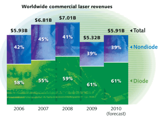 c indicators were so dire in the latter part of 2008 that Laser Focus World-anticipating
laser sales to remain flat or decrease as much as 20%, depending on the market
sector-forecast an overall 11.3% drop in the worldwide laser markets to $6.32 billion
(see www.laserfocusworld.com/articles/349353). But by early 2009, it was
obvious that the chasm would be even deeper. According to our annual survey,
actual laser sales for 2009 were $5.32 billion-a 24.1% drop from the $7.01
billion for 2008, setting sales back to 2003 levels. And if Main Street is any
indication (forget the "subsidized" rally on Wall Street), this deep
chasm is also wide. Even though the U.S. unemployment rate dropped to 10.0% in
November 2009 from its 10.2% high (a jobless recovery), many economists predict
that it could be three years before jobs return and sales improve to pre-2008
levels. c indicators were so dire in the latter part of 2008 that Laser Focus World-anticipating
laser sales to remain flat or decrease as much as 20%, depending on the market
sector-forecast an overall 11.3% drop in the worldwide laser markets to $6.32 billion
(see www.laserfocusworld.com/articles/349353). But by early 2009, it was
obvious that the chasm would be even deeper. According to our annual survey,
actual laser sales for 2009 were $5.32 billion-a 24.1% drop from the $7.01
billion for 2008, setting sales back to 2003 levels. And if Main Street is any
indication (forget the "subsidized" rally on Wall Street), this deep
chasm is also wide. Even though the U.S. unemployment rate dropped to 10.0% in
November 2009 from its 10.2% high (a jobless recovery), many economists predict
that it could be three years before jobs return and sales improve to pre-2008
levels.
(Click the image to read the full article on www.optoiq.com) Image: Laser Focus World
|
Fire-Rated Glass Forecast
Katy Devlin, Glass Magazine, January 7, 2010
Safti
First, San Francisco, supplied its SuperLite II-XL 120 in GPX Framing for
Ohio's Cleveland Clinic.
Nonresidential construction
spending is expected to fall 5 percent in 2010, following a 5.7 percent loss in
2009, and isn't expected to rebound until 2011, according to Jim Haughey, chief
economist, Reed Construction Data, Norcross, Ga. Despite
the grim forecast, representatives from fire-rated glazing suppliers remain
optimistic. The market segment is partly insulated from the downturn thanks to
code requirements, building trends and increased funding for some public
projects, they say.
"Although we are currently experiencing a very soft market in the commercial
construction industry, demand for non-wired fire-rated glazing products
continues to grow," says Dan Poling, sales manager, fire rated glass products, Schott North America Inc., Elmsford, N.Y. Poling attributes the growth to
adoption of International Building Codes nationwide. currently experiencing a very soft market in the commercial
construction industry, demand for non-wired fire-rated glazing products
continues to grow," says Dan Poling, sales manager, fire rated glass products, Schott North America Inc., Elmsford, N.Y. Poling attributes the growth to
adoption of International Building Codes nationwide.
(Click the image to read the full article on www.glassmagazine.com) Image: Glass Magazine
|
|
Braincake
is Established to Help Girls Learn Science and Math
 A
partnership program at Carnegie Science Center called Braincake.org is set up
to help girls, age 11-17, learn math and science. This program encourages more
girls to enter science and engineering fields of study. As many of our readers know, we are
experiencing a shortage of younger science majors especially females. This work
is cosponsored by the Alcoa Foundation, The Comcast Foundation, Google,
Comcast, Dragonfly TV and First Commonwealth. Use the link below to visit the Braincake website. Also,
they are on Facebook at GMSP Girls of Math and Science Partnership. A
partnership program at Carnegie Science Center called Braincake.org is set up
to help girls, age 11-17, learn math and science. This program encourages more
girls to enter science and engineering fields of study. As many of our readers know, we are
experiencing a shortage of younger science majors especially females. This work
is cosponsored by the Alcoa Foundation, The Comcast Foundation, Google,
Comcast, Dragonfly TV and First Commonwealth. Use the link below to visit the Braincake website. Also,
they are on Facebook at GMSP Girls of Math and Science Partnership.
(click the image to link to www.braincake.org) Image: www.braincake.org
|
Photonics Applied: Optical biomimetics emerge from a deep, dark past
Andrew Parker, Laser Focus World, January 1, 2010
"In
the country of the blind, the one-eyed man is king." This famous dictum
from H. G. Wells tells us something that may seem self-evident: sight matters.
But imagine for a moment that the country of the blind is in fact the whole
world, 521 million years ago. It's a world in which life is primitive and
aimless, and evolution slow and painstaking.
 Then
something remarkable happens. Over the next million years,Biomimetics the
process of evolution kicks into overdrive. For the first time, animals evolve
hard external parts. Both hunters and prey develop armaments and defenses. So
in this short space of time-the blink of an eye in geological terms-all animals
on Earth, no matter how unrelated, leave their soft skins behind. When I traced
back the origin of vision, I found that the first image-forming eye evolved in
a predatory animal (one that could have an impact on others) around 521 million
years ago, precisely at the beginning of this Big Bang of evolution. Hence
vision appears to have lit the fuse for life's explosion. Then
something remarkable happens. Over the next million years,Biomimetics the
process of evolution kicks into overdrive. For the first time, animals evolve
hard external parts. Both hunters and prey develop armaments and defenses. So
in this short space of time-the blink of an eye in geological terms-all animals
on Earth, no matter how unrelated, leave their soft skins behind. When I traced
back the origin of vision, I found that the first image-forming eye evolved in
a predatory animal (one that could have an impact on others) around 521 million
years ago, precisely at the beginning of this Big Bang of evolution. Hence
vision appears to have lit the fuse for life's explosion.
But
why is this important to the photonics community? Because with those first hard
parts in animals came the first photonic nanostructures on Earth. With the
evolution of the eye, the size, shape, color, and behavior of animals were
suddenly revealed for the first time. The animal kingdom exploded into life.
Color was among their main weapons. And from that moment until today, color on
Earth has functioned to provide camouflage and crypsis, as well as warning
colors and mating colors to attract the eye...
Click the image to read the full article on www.optoiq.com)
|
Heavy Elements: International
body dubs element 112 Copernicium
Mitch Jacoby, Chemical and Engineering News, February 26, 2010
The periodic table officially has a new entry. The International Union of Pure & Applied Chemistry announced its approval last week of the name copernicium and symbol Cn for element 112 (Pure
Appl. Chem., DOI: 10.1351/PAC-REC-09-08-20).
The approval follows IUPAC's extensive
review of claims made by the GSI Helmholtz Center for Heavy Ion Research, in
Darmstadt, Germany, of being the first team to synthesize element 112. GSI's
claims date back to 1996. IUPAC's announcement raises to six the total number
of elements officially discovered and named by GSI.
GSI team leader Sigurd Hofmann
explains that his team's intention in selecting the name for element 112 is "to
salute Nicolaus Copernicus, an influential scientist who didn't receive any
accolades in his own lifetime, and to highlight the link between astronomy and
the field of nuclear chemistry." Copernicus was the 16th-century Polish astronomer
who developed the sun-centered model of the solar system-a radical departure
from the thinking that prevailed in Copernicus' day.
The Darmstadt researchers have
previously been recognized for the discovery of five other elements, which they
named bohrium (107), hassium (108), meitnerium (109), darmstadtium (110), and
roentgenium (111).
(click here to read the full article www.pubs.acs.org)
|
Mechanical Devices Stamped on Plastic
Larry Hardesty, MIT News, February 26, 2010
Microelectromechanical
devices - tiny machines with moving parts - are everywhere these days: they
monitor air pressure in car tires, register the gestures of video game players,
and reflect light onto screens in movie theaters. But they're manufactured the
same way computer chips are, in facilities that can cost billions of dollars,
and their rigidity makes them hard to wrap around curved surfaces.
 MIT researchers have discovered a way to make microelectromechanical devices,
or MEMS, by stamping them onto a plastic film. That should significantly reduce
their cost, but it also opens up the possibility of large sheets of sensors
that could, say, cover the wings of an airplane to gauge their structural
integrity. The printed MEMS are also flexible, so they could be used to make
sensors with irregular shapes. And since the stamping process dispenses with
the harsh chemicals and high temperatures ordinarily required for the
fabrication of MEMS, it could allow MEMS to incorporate a wider range of
materials. MIT researchers have discovered a way to make microelectromechanical devices,
or MEMS, by stamping them onto a plastic film. That should significantly reduce
their cost, but it also opens up the possibility of large sheets of sensors
that could, say, cover the wings of an airplane to gauge their structural
integrity. The printed MEMS are also flexible, so they could be used to make
sensors with irregular shapes. And since the stamping process dispenses with
the harsh chemicals and high temperatures ordinarily required for the
fabrication of MEMS, it could allow MEMS to incorporate a wider range of
materials.
Conventional MEMS are built through a process called photolithography, in which
different layers of material are chemically deposited on a substrate - usually
a wafer of some semiconducting material - and etched away to form functional
patterns. Since a wafer is at most 12 inches across, arranging today's MEMS
into large arrays requires cutting them out and bonding them to some other
surface.
(Click the image to
read the full article on MITnews) Image: Corinne Packard and Apoorva
Muraka
|
|
SVC Announces Three New Tutorial Courses Featured at the 2010 TechCon in Orlando, FL
| |
 Interested in sharing the latest news in vacuum coating technology? Forward us a link to an article you want to share with the rest of the SVC readership to publications@svc.org. Purchase advertising space on this newsletter by contacting SVC at svcinfo@svc.org. Interested in sharing the latest news in vacuum coating technology? Forward us a link to an article you want to share with the rest of the SVC readership to publications@svc.org. Purchase advertising space on this newsletter by contacting SVC at svcinfo@svc.org. |
Society of Vacuum Coaters 71 Pinon Hill Place, NE
Albuquerque, NM 87122
(505) 856-7188 Fax (505) 856-6716
www.svc.org E-mail: svcinfo@svc.org
|
|
|